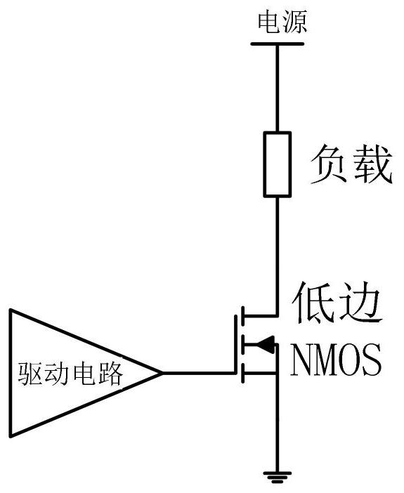
Driving circuit of low-side NMOS (N-channel metal oxide semiconductor)
- Summary
- Abstract
- Description
- Claims
- Application Information
AI Technical Summary
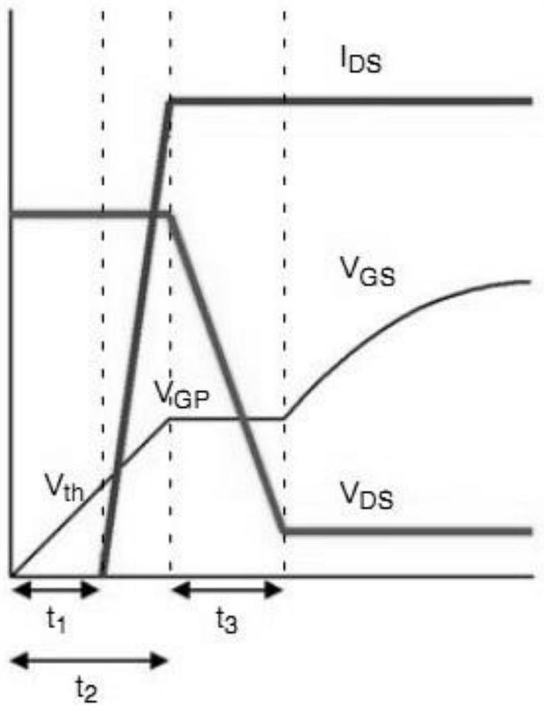
Problems solved by technology
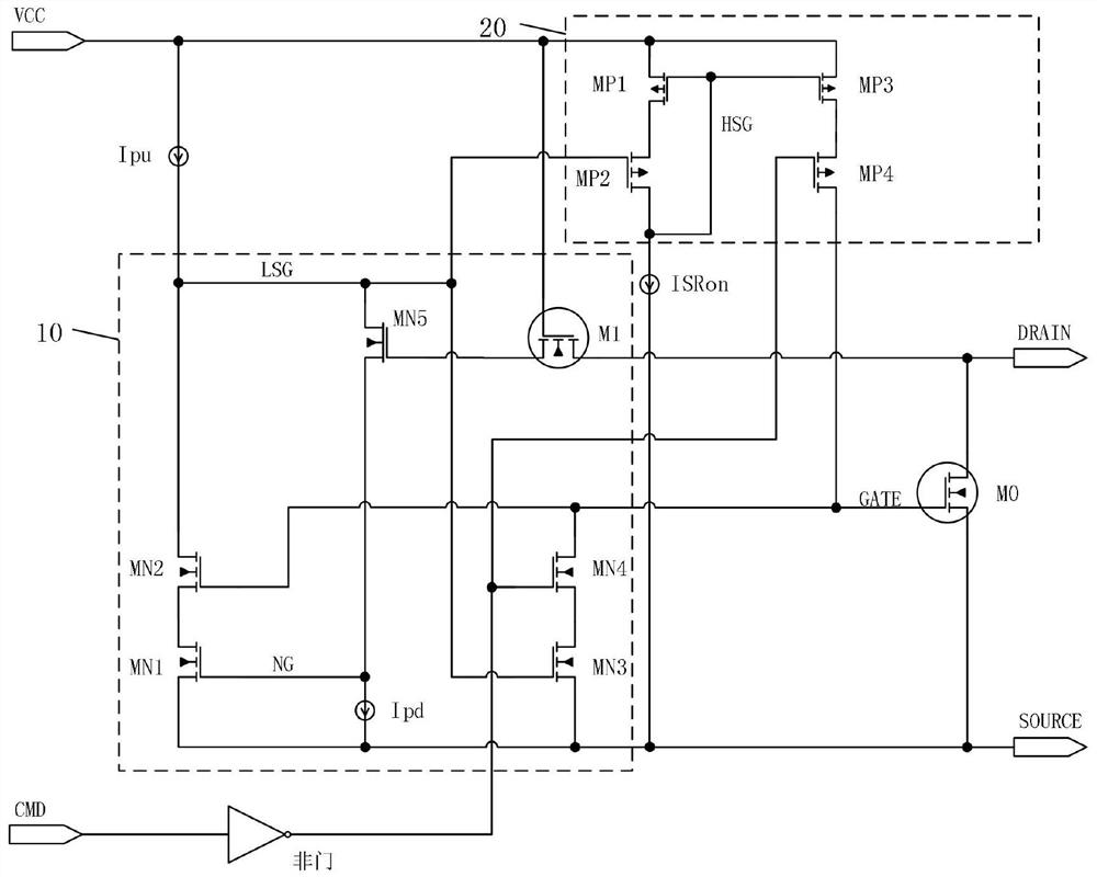
Method used
Image

Examples
Embodiment Construction
[0058]In order to make the purpose, technical solutions and advantages of the embodiments of the present invention clearer, the technical solutions in the embodiments of the present invention will be clearly and completely described below in conjunction with the drawings in the embodiments of the present invention. Obviously, the described embodiments It is a part of embodiments of the present invention, but not all embodiments. Based on the embodiments of the present invention, all other embodiments obtained by persons of ordinary skill in the art without making creative efforts belong to the protection scope of the present invention.
[0059] In this application, the term "comprises", "comprises" or any other variation thereof is intended to cover a non-exclusive inclusion such that a process, method, article, or apparatus comprising a set of elements includes not only those elements, but also includes none. other elements specifically listed, or also include elements inhere...
PUM
 Abstract
Description
Claims
Application Information