
OLED display, preparation method thereof, and QLED display

A display and device technology, applied in the field of OLED display and its preparation, and QLED display, can solve the problems of uneven film formation, complex process, low luminous efficiency, etc., and achieve the goal of reducing the difficulty of the preparation process, improving the preparation efficiency, and shortening the process steps. Effect

Pending Publication Date: 2021-11-26
南京芯视元电子有限公司
View PDF0 Cites 0 Cited by
  • Summary
  • Abstract
  • Description
  • Claims
  • Application Information

AI Technical Summary

Problems solved by technology

However, this way of using the subsequent anodization process, on the one hand, the process is complex, and the thermal expansion coefficient, functional function, and lattice parameters between the materials of each layer need to be considered during the deposition process to avoid film formation. Problems such as unevenness, shedding, or low luminous efficiency; secondly, due to the small pixel size of OLED displays, subsequent manufacturers need to separately formulate yellow light processes based on CMOS drive circuit substrates to make suitable OLED device anodes, which makes Invisibly increased production costs

Method used


Image

  • OLED display, preparation method thereof, and QLED display
  • OLED display, preparation method thereof, and QLED display
  • OLED display, preparation method thereof, and QLED display

Examples


Embodiment Construction

[0027] The embodiments described below represent the information necessary to practice the embodiments in the art, and the best mode of the embodiment is shown. After reading the following description with reference to the drawings, those skilled in the art will understand the concepts of the present disclosure and will recognize the applications of these concepts not specifically proposed herein. It should be understood that these concepts and applications are within the scope of the present disclosure and the appended claims.

[0028] It should be understood that although the terms first, second, the second, etc. can be used herein, but these components should not be limited by these terms. These terms are only used in the area to divide one component and another element. For example, the first element can be referred to as a second element without departing from the scope of the present disclosure, and similarly, the second element can be referred to as the first element. As us...


PUM

PropertyMeasurementUnit
Thicknessaaaaaaaaaa

Abstract

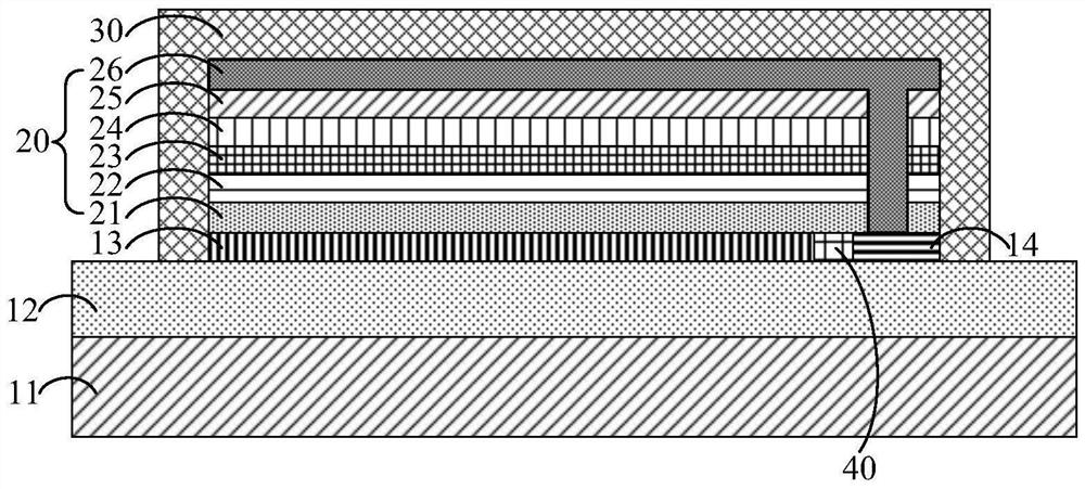
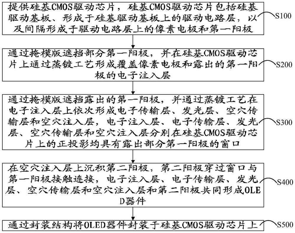
The invention discloses an OLED display, a preparation method thereof and a QLED display, and relates to the technical field of display. The OLED display comprises a silicon-based CMOS driving chip, an OLED device and a packaging structure used for packaging the OLED device on the silicon-based CMOS driving chip, the silicon-based CMOS driving chip comprises a silicon-based driving substrate, a driving circuit layer located on the silicon-based driving substrate, and a pixel electrode and a first anode which are arranged on the driving circuit layer at an interval; the OLED device comprises at least one light-emitting layer located on the pixel electrode and a second anode located on the light-emitting layer and in ohmic contact with the first anode; and the pixel electrode serves as a cathode of the OLED device, and light beams emitted by the self-luminous layer sequentially penetrate through the second anode and the packaging structure to be emitted. The OLED display does not need an anodizing process, so that the process yield can be improved, and the process steps can be shortened.

Description

Technical field [0001] The present disclosure relates to the field of display, in particular, to an OLED display and a preparation method thereof, a QLED display. Background technique [0002] Silicon-based OLED (Organic Light Emitting Diode, Organic Light Emitting Diode) Micro Display is a new type of display technology that makes an active light emitting device OLED on a silicon-based CMOS drive chip. Because of its high integration, micron-sized pixel size, and low power consumption, it is well received in the field of near-eye display. At present, the silicon-based OLED micro displays have been widely used in the military sector of guns, night vision and machine helmets and consumer electronic fields represented by Ar / VR, which can bring unprecedented visual experience to users, known as A generation of black horses showing technology. [0003] The top-level process metal of the conventional CMOS drive circuit substrate generally has only metal aluminum, tungsten and titani...

Claims


Application Information

Patent Timeline
IPC IPC(8): H01L27/32H01L51/52H01L51/56
CPCH10K59/12H10K50/81H10K50/82H10K59/1201H10K71/00
Inventor 朱舒卷何军
Owner 南京芯视元电子有限公司
Learn More