Annealing method of semiconductor laser

A technology of lasers and semiconductors, applied in semiconductor lasers, lasers, laser components, etc., can solve problems such as high stress of semiconductor lasers, achieve the effect of optimizing temperature difference stress and improving beam quality

Pending Publication Date: 2021-11-30
XI'AN POLYTECHNIC UNIVERSITY
View PDF0 Cites 0 Cited by
  • Summary
  • Abstract
  • Description
  • Claims
  • Application Information

AI Technical Summary

Problems solved by technology

[0003] The purpose of the present invention is to provide a semiconductor laser annealing method, which solves t

Method used


Image

  • Annealing method of semiconductor laser
  • Annealing method of semiconductor laser
  • Annealing method of semiconductor laser

Examples


Example Embodiment

[0020] The present invention will be described in detail below with reference to the accompanying drawings and specific embodiments.
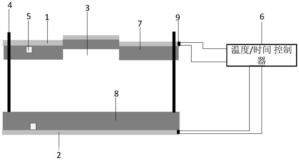
[0021] An annealing method for a semiconductor laser for indium encapsulating cooling semiconductor laser bar annealing, and a solder, chip is provided with solder, chip, including the following steps:

[0022] Using annealing device, annealing device includes a first jig 7, a second clamp 8, a laser heat sink between the first clamp 7, the second clamp 8, the first clamp 7, the second clamp 8 is distinguished from the heat sinking surface There is a first temperature regulator 1, the second temperature regulator 2, the first temperature regulator 1, and the second temperature regulator 2 are fixed to the first clamp 7, the second clamp 8, respectively, the thickness of the temperature regulator is negligible. The material of the clamp is consistent with the heat sink material. The first temperature regulator 1, the second temperature regulator 2 s...


PUM


Abstract

The invention discloses an annealing method of a semiconductor laser, which comprises the steps that an annealing device is adopted, the annealing device comprises a first clamp and a second clamp, a laser heat sink is located between the first clamp and the second clamp, and a first temperature regulator and a second temperature regulator are respectively arranged on the surfaces, far away from the laser heat sink, of the first clamp and the second clamp; stepped constant-speed annealing is carried out on the upper surface and the lower surface of the heat sink at the same time, the temperature difference stress of the clamp and the heat sink in the thickness direction is optimized, chip warping generated by the temperature difference stress in the thickness direction and chip warping caused by CTE mismatching of the chip and the heat sink are eliminated, and the purpose of eliminating semiconductor laser smile in the packaging process and the laser beam quality is improved are achieved.

Description

technical field [0001] The invention belongs to the technical field of semiconductor lasers and relates to an annealing method for semiconductor lasers. Background technique [0002] Semiconductor lasers are small in size, long in life, and can be pumped by simple injection of current. Their operating voltage and current are compatible with integrated circuits and can be integrated monolithically. Therefore, semiconductor lasers have been widely used in laser processing, laser weapons, laser communications, optical storage, optical gyro, laser printing, ranging and radar. Semiconductor lasers are required to have high beam quality and high brightness in many application fields. During the packaging process, the semiconductor laser produces a smile effect due to thermal stress, which reduces the beam quality and brightness of the device. At present, the single-side annealing method is mainly used in the annealing process of semiconductor lasers, and this method is annealed ...

Claims


Application Information

Patent Timeline
IPC IPC(8): H01S5/022H01S5/0235
CPCH01S5/022H01S5/0235
Inventor 熊玲玲杨鹏程刘晖和丹
Owner XI'AN POLYTECHNIC UNIVERSITY
Why Eureka
Try Eureka