High-precision multi-dimensional adjustment alignment system and method for optical fiber sensor packaging

An optical fiber sensor and multi-dimensional adjustment technology, which is applied in the direction of instruments, measuring devices, scientific instruments, etc., can solve the problems that the coating surface is easy to turn over, hard to put down, and affect production efficiency, etc., to achieve short alignment adjustment time, accurate adjustment alignment, The effect of improving productivity

Pending Publication Date: 2021-12-10
西安和其光电科技股份有限公司
View PDF0 Cites 0 Cited by
  • Summary
  • Abstract
  • Description
  • Claims
  • Application Information

AI Technical Summary

Problems solved by technology

[0006] In order to solve the coupling between the existing semiconductor chip and the end face of the optical fiber, the chip is easy to be scratched, the coated surface is easy to turn over and the surface is easy to attach dirt, and it is difficult to put it down after clamping; and it takes a long time to replace the chip and adjust the alignment. , a technical problem that affects production efficiency, the present invention provides a high-precision multi-dimensional adjustment alignment system and method for optical fiber sensor packaging

Method used


Image

  • High-precision multi-dimensional adjustment alignment system and method for optical fiber sensor packaging
  • High-precision multi-dimensional adjustment alignment system and method for optical fiber sensor packaging
  • High-precision multi-dimensional adjustment alignment system and method for optical fiber sensor packaging

Examples


Embodiment Construction

[0054] The content of the present invention will be further described in detail below in conjunction with the accompanying drawings and specific embodiments.

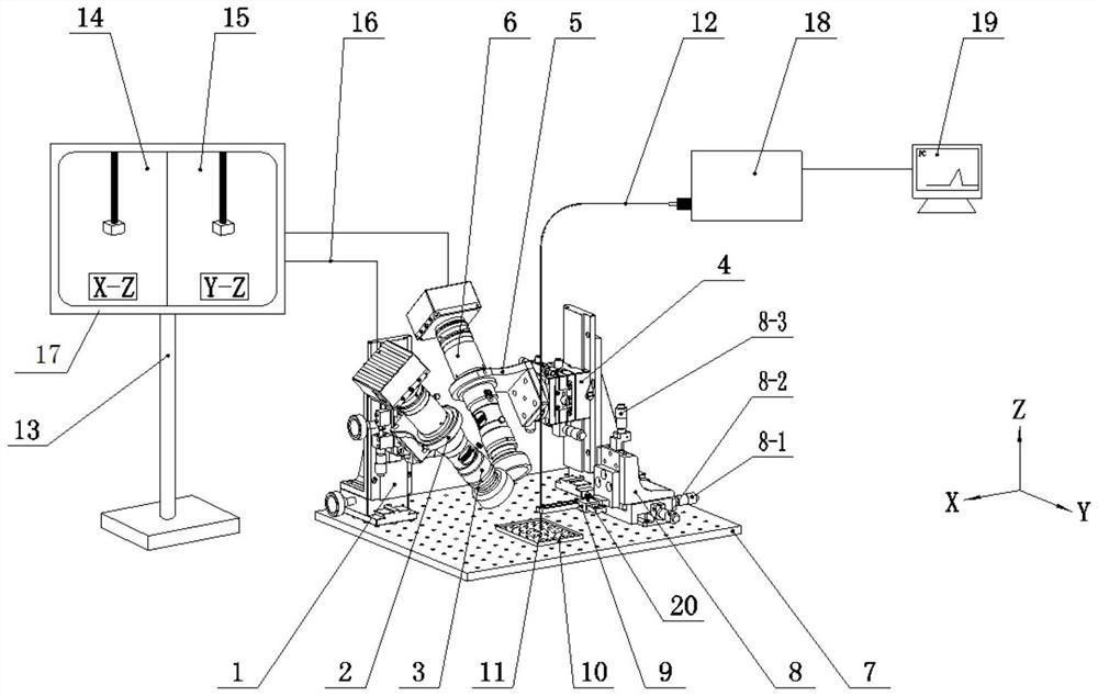
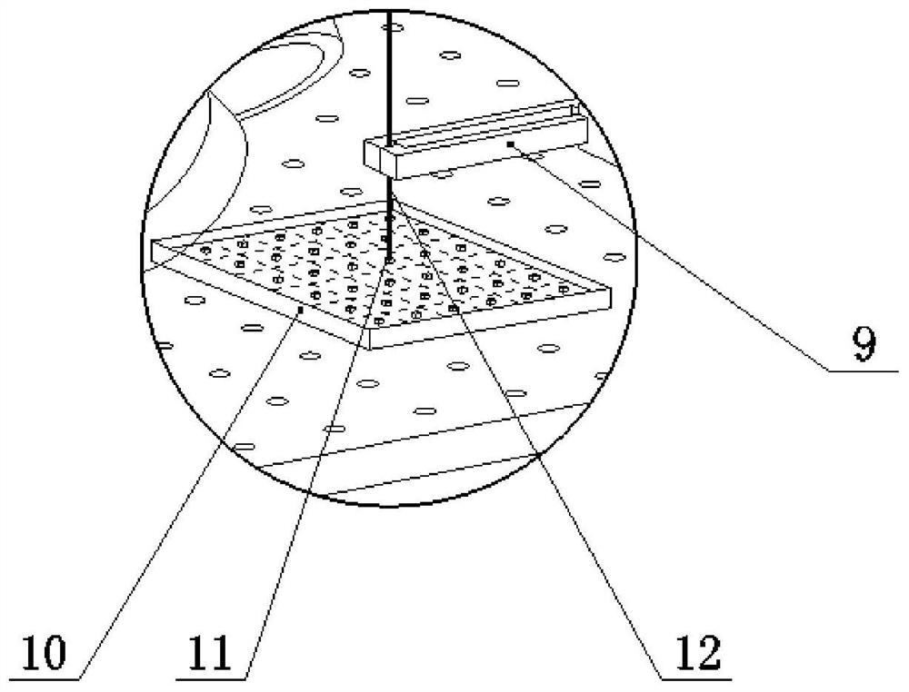
[0055] Such as figure 1 and figure 2 As shown, the present invention is a high-precision multi-dimensional adjustment and alignment system for optical fiber sensor packaging, including an optical platform 7, a wafer adsorption magazine 10, an optical fiber clamping assembly 9, a first alignment unit, a second alignment unit, Display unit 17 and spectrum monitoring unit.

[0056] The wafer adsorption material box 10 is arranged on the optical table 7, and the material of the wafer adsorption material box 10 is silica gel; the wafer adsorption material box 10 is used to place the semiconductor wafer 11 to be packaged, and the thin silica gel layer in the wafer adsorption material box 10 is opposite to the semiconductor wafer. 11 Natural adsorption and fixation, and after the optical fiber and semiconductor wafer are ac...


PUM


Abstract

The invention provides a high-precision multi-dimensional adjustment alignment system and method for optical fiber sensor packaging, and solves the problems that when an existing semiconductor wafer is coupled with an optical fiber, the wafer is easy to scratch, a film coating surface is easy to overturn, dirt is easy to attach to the surface, the wafer is difficult to put down after being clamped, and the time consumed for alignment adjustment is long. The system comprises an optical platform, a wafer adsorption material box, an optical fiber clamping assembly, a display unit, a spectrum monitoring unit, a first adjusting base, a second adjusting base, a first camera assembly and a second camera assembly, wherein the first adjusting base and the second adjusting base are arranged on the optical platform; the first camera assembly is arranged on the first adjusting base; the second camera assembly is arranged on the second adjusting base; the wafer adsorption material box is arranged on the optical platform; the optical fiber clamping assembly is arranged on the optical platform through a three-dimensional adjusting frame; the plane where the upper surface of the wafer adsorption material box is located is an XY plane; the display unit comprises an X-Z display interface and a Y-Z display interface which are respectively connected with the first camera assembly and the second camera assembly; and the spectrum monitoring unit comprises a signal coupling monitoring module and an upper computer connected with the signal coupling monitoring module.

Description

technical field [0001] The invention relates to the field of optical fiber sensor packaging, in particular to a high-precision multi-dimensional adjustment alignment system and method for optical fiber sensor packaging. Background technique [0002] Semiconductor materials have absorption bands for the spectrum, and, as the temperature increases, the absorption spectrum bands red shift. With this principle, accurate temperature measurement can be realized. Optical fiber sensing and temperature measurement can be realized by precisely coupling the cut semiconductor wafer with the optical fiber and monitoring the shift of the absorption spectral band of the semiconductor material. The precise coupling of the semiconductor wafer and the end face of the optical fiber is a key process for the packaging of the optical fiber sensor. Since the core diameter of the optical fiber and the size of the dicing wafer are very small, it is difficult to precisely clamp the dicing wafer. In...

Claims


Application Information

Patent Timeline
IPC IPC(8): G01K11/32
CPCG01K11/32
Inventor 樊维涛单娟李跟兴翟凯旋郑皓文
Owner 西安和其光电科技股份有限公司
Why Eureka
Try Eureka