Multi-channel super-junction IGBT device

A multi-channel, device technology, applied in the direction of semiconductor devices, semiconductor/solid-state device manufacturing, electrical components, etc., can solve the problems of increasing system cost and complexity, device burnout, current oscillation, etc., to improve anti-EMI ability and prevent current Oscillation, the effect of reducing conduction loss

Pending Publication Date: 2021-12-10
SHANGHAI SUPERSEMICONDUCTOR TECH CO LTD
View PDF0 Cites 0 Cited by
  • Summary
  • Abstract
  • Description
  • Claims
  • Application Information

AI Technical Summary

Problems solved by technology

Smaller chip area leads to smaller gate input capacitance. When super-junction IGBT devices are used to replace traditional IGBT devices, the strong drive current of the driver chip will cause super-junction IGBT devices to easily form current oscillations when they are turned on, resulting in EMI problems. Even cause the device to burn
Therefore, super-junction IGBT devices cannot directly replace traditional IGBT devices when they are applied. It is necessary to adjust the peripheral circuit or replace the driver chip with a smaller driving current, which indirectly increases the system cost and complexity of the application solution provider.

Method used


Image

  • Multi-channel super-junction IGBT device
  • Multi-channel super-junction IGBT device
  • Multi-channel super-junction IGBT device

Examples


Embodiment Construction

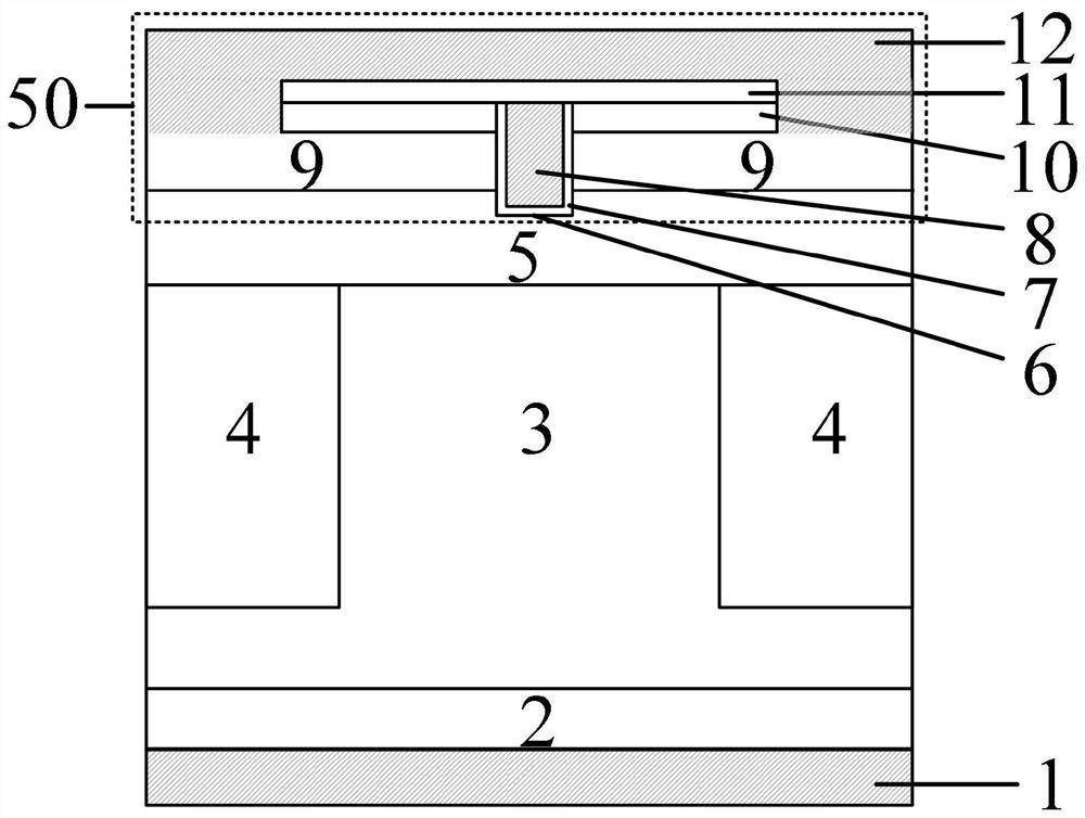
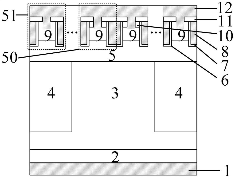
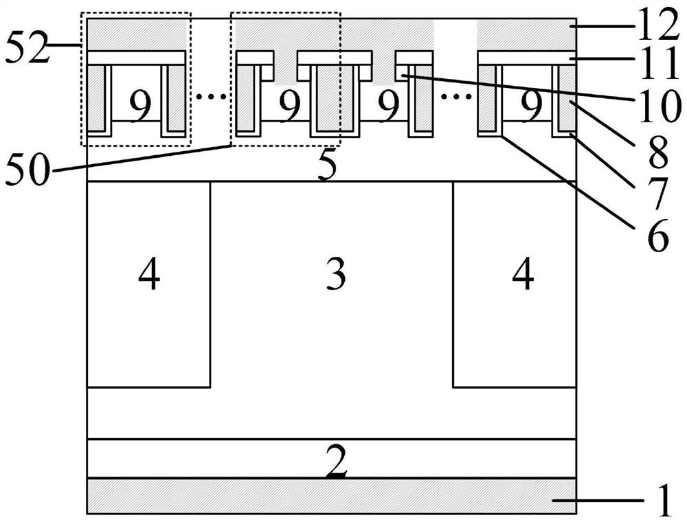
[0025] In order to make the purpose, technical solution and advantages of the present invention clearer, the technical solution of the present invention will be fully described below in a specific manner in conjunction with the drawings in the embodiments of the present invention. Apparently, the described embodiments are some embodiments of the present invention, rather than all embodiments. Based on the embodiments of the present invention, all other embodiments obtained by persons of ordinary skill in the art without making creative efforts, All fall within the protection scope of the present invention. The principles and features of the present invention will be described below in conjunction with the accompanying drawings. The examples given are only for the present invention at that time, and are not used to limit the scope of the present invention.

[0026] It should be understood that terms such as "having", "comprising" and "including" used herein do not denote the pre...


PUM

PropertyMeasurementUnit
electrical resistivityaaaaaaaaaa
thicknessaaaaaaaaaa
thicknessaaaaaaaaaa

Abstract

The invention provides a multi-channel super-junction IGBT device. The device comprises a metalized collector electrode, a P- substrate, a first N-type epitaxial layer and a second N-type epitaxial layer, wherein the first N-type epitaxial layer is positioned above the P-substrate, and the second N-type epitaxial layer is positioned above the first N-type epitaxial layer; and the second N epitaxial layer at least comprises a first virtual MOS cellular unit and an MOS cellular unit, and the first virtual MOS cellular unit comprises a groove formed through reactive ion etching, a thermally grown gate oxide layer arranged in the groove and deposited heavily doped polycrystalline silicon located in the gate oxide layer. According to the device structure disclosed by the invention, the cellular size limitation of the PN column pitch of a traditional super-junction IGBT device is broken through, the number of the top layer MOS cells and the number of the virtual MOS cells can be increased or decreased according to the application requirements of the device so as to adjust the gate input capacitance of the super-junction IGBT device, current oscillation when the device is started is prevented, and the EMI resistance of the device is improved. And meanwhile, the device also has the characteristics of adjusting saturation output current density, forward conduction voltage drop and short-circuit time tolerance.

Description

technical field [0001] The invention belongs to the technical field of power semiconductor devices, and in particular relates to a multi-channel super-junction IGBT device. Background technique [0002] A conventional super junction IGBT (Insulated Gate Bipolar Transistor) device structure in the prior art is as follows figure 1 As shown, it includes a metallized collector electrode 1, a P-type substrate 2, a first N-type epitaxial layer 3 located above the P-type substrate 2, and a P Column 4, the second N epitaxial layer 5 located above the first N type epitaxial layer 3 and P column 4, there is only one MOS cell 50 in the second N type epitaxial layer 5, and the MOS cell 50 includes trench 6, a thermally grown gate oxide layer 7, deposited heavily doped polysilicon 8, and a P-type body region 9 formed by a self-aligned process, and the P-type body region 9 is provided with partially independent N+ Source region 10, deposited borophosphosilicate glass 11, metallized emit...

Claims


Application Information

Patent Timeline
Patent Type & Authority Applications(China)
IPC IPC(8): H01L29/06H01L29/739H01L21/331
CPCH01L29/0634H01L29/0696H01L29/7397H01L29/66348H01L23/552H01L29/0607H01L29/1095H01L29/1608H01L29/20
Inventor 吴玉舟李菲李欣刘铁川禹久赢
Owner SHANGHAI SUPERSEMICONDUCTOR TECH CO LTD
Why Eureka
Try Eureka