Mini LED wafer appearance defect detection system and method
A detection system and a technology for appearance defects, applied in the field of defect detection, can solve the problems of low detection efficiency, inconsistent standards, complex production processes, etc., and achieve the effects of reducing production costs, improving accuracy, and improving work efficiency
- Summary
- Abstract
- Description
- Claims
- Application Information
AI Technical Summary
Problems solved by technology
Method used
Image
Examples
Embodiment 1
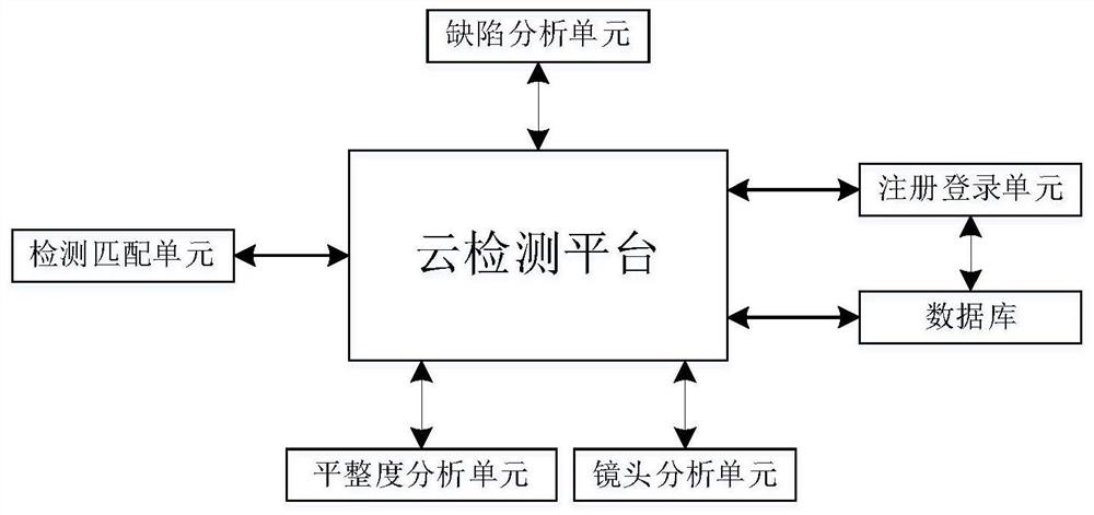
[0102] A Mini LED wafer appearance defect detection system, including high magnification and high numerical aperture lens, large target surface high resolution camera, light source, displacement stage, computer image processing system; large target surface high resolution camera and high magnification high numerical aperture lens In cooperation, the high magnification and high numerical aperture lens is set under the high resolution camera with a large target surface, and the displacement stage is set directly under the high magnification and high numerical aperture lens during detection; the lens adopts a high magnification and high numerical aperture lens with a magnification of 3 times or more. It can clearly image defects of 0.5μm-200μm on the surface of the Mini-LED, and effectively distinguish and screen out products with appearance defects; the high-resolution camera with a large target surface is a high-resolution camera with a large target surface of 4 / 3inch or more; Mi...
Embodiment 2
[0104] Carry out the loading operation, and use the fixed module to adsorb and fix the wafer sample to be tested on the sample carrier; adopt n2 partition method for the wafer, where n is a positive integer; use the X / Y axis displacement module to place the wafer The sample is accurately moved to the ranging area, and the representative chip in each partition is measured in sequence according to the preset partition track, and the ranging value in each partition is calculated and processed to obtain the average value of the ranging deviation of the partition ;After completing the partition ranging operation, use the X / Y axis displacement module to accurately move the wafer sample to the imaging area, and use the vision device to sequentially image each partition chip according to the preset partition track. The industrial lens of the vision device When the field of view enters a partition for the first time, first use the absolute value of the mean value of the ranging deviati...
PUM
 Abstract
Description
Claims
Application Information
 - R&D Engineer
- R&D Manager
- IP Professional
- Industry Leading Data Capabilities
- Powerful AI technology
- Patent DNA Extraction
Browse by: Latest US Patents, China's latest patents, Technical Efficacy Thesaurus, Application Domain, Technology Topic, Popular Technical Reports.
© 2024 PatSnap. All rights reserved.Legal|Privacy policy|Modern Slavery Act Transparency Statement|Sitemap|About US| Contact US: help@patsnap.com


