Laser marking method of silicon wafer and manufacturing method of heterojunction cell

A laser marking method and technology for heterojunction cells, which are used in photovoltaic power generation, manufacturing tools, laser welding equipment, etc., can solve the problems of silicon wafer damage and affect the performance of heterojunction cells, and achieve good electrical performance and battery conversion High efficiency and reduce mechanical damage

Pending Publication Date: 2021-12-21
宣城睿晖宣晟企业管理中心合伙企业(有限合伙)
View PDF0 Cites 1 Cited by
  • Summary
  • Abstract
  • Description
  • Claims
  • Application Information

AI Technical Summary

Problems solved by technology

[0004] Therefore, the technical problem to be solved by the present invention is to overcome the defects in the prior art that laser marking on silicon wafers is easy to cause damage to silicon wafers, thereby affecting the performance of heterojunction cells, thereby providing a laser marking method for silicon wafers And the manufacturing method of heterojunction battery

Method used


Image

  • Laser marking method of silicon wafer and manufacturing method of heterojunction cell
  • Laser marking method of silicon wafer and manufacturing method of heterojunction cell
  • Laser marking method of silicon wafer and manufacturing method of heterojunction cell

Examples


Embodiment 1

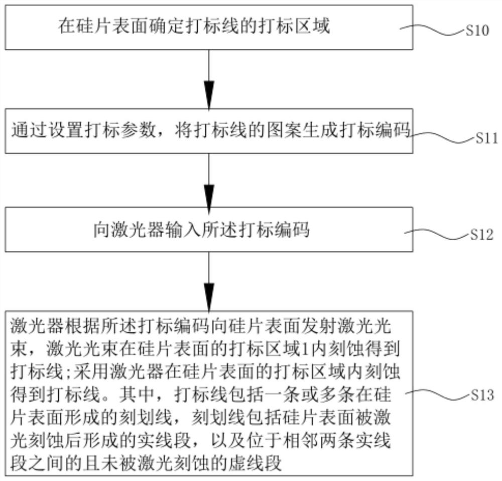
[0044]A silicon wafer laser marking method is exemplified by combining the silicon wafer laser marking method with the application of silicon wafers in the manufacture of heterojunction cells. combine figure 1 As shown in -2, a laser marking method for a silicon wafer includes the following steps:

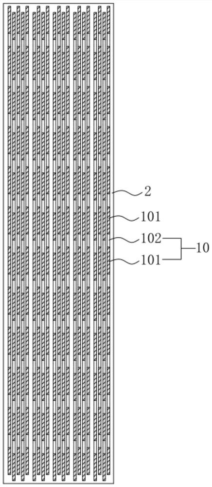
[0045] Step S10: Determine the marking area 1 of the marking line on the surface of the silicon wafer 2.

[0046] Specifically, when determining the marking area 1, the marking line should be located as far as possible under the auxiliary gate line 4 after the silicon wafer 2 is made into a heterojunction cell, avoiding the position of the main grid line 3; and the size of the marking area 1 is 5mm2-30mm 2 , the distance between the marking line in the marking area 1 and the edge of the silicon wafer 2 is kept between 1mm-3mm. Marking area 1 is as close to the edge of silicon wafer 2 as possible to reduce the influence of laser marking on grid lines during screen printing, other...

Embodiment 2

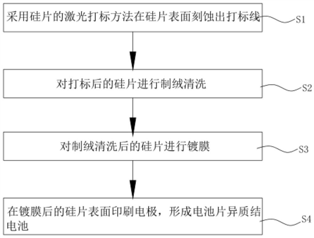
[0059] combine image 3 and Figure 4 As shown, Embodiment 2 of the present invention provides a method for manufacturing a heterojunction battery, including the following steps:

[0060] Step S1, using the laser marking method for silicon wafers in the above-mentioned embodiment 1 to etch a marking line on the surface of the silicon wafer; Step S2, performing texturing cleaning on the marked silicon wafer 2; Step S3, cleaning the texturing The finished silicon wafer 2 is coated; step S4, printing electrodes on the surface of the coated silicon wafer 2 to form a heterojunction cell.

[0061] In this embodiment, the fabricated heterojunction battery is a silicon-based heterojunction heterojunction battery, and the coating process includes a PECVD coating process and an ITO film coating process performed in sequence. When the heterojunction heterojunction cell uses the N side as the light incident surface, the marking line needs to be marked on the N side; when the heterojunct...


PUM

PropertyMeasurementUnit
wavelengthaaaaaaaaaa

Abstract

The invention discloses a laser marking method of a silicon wafer and a manufacturing method of a heterojunction cell. The laser marking method comprises the steps: enabling a pattern of a marking line to generate a marking code through setting marking parameters; inputting the marking code to a laser; and the laser being used to emit light beams to the surface of the silicon wafer according to the marking code, and the light beams being used to etch the surface of the silicon wafer to obtain the marking line. The marking line comprises a scribing line formed on the surface of the silicon wafer, and the scribing line comprises a solid line segment formed after the surface of the silicon wafer is etched by the laser and a dotted line segment which is not etched by the laser. According to the laser marking method, the mechanical damage to the silicon wafer in the laser marking process can be reduced to the greatest extent, the damaged surface formed on the silicon wafer is relatively smooth, and the silicon wafer does not have a shadow under PL imaging; and after the heterojunction cell is prepared, the electric leakage phenomenon at the laser code printing position is less, the electrical property is better, and the cell conversion efficiency is high. In addition, after the silicon wafer is textured and cleaned, a pyramid textured surface can be formed at the etching position, so that the influence of the silicon wafer on light absorption is avoided.

Description

technical field [0001] The invention relates to the technical field of heterojunction batteries, in particular to a laser marking method for silicon wafers and a manufacturing method for heterojunction batteries. Background technique [0002] At present, laser equipment is generally used to write and code on silicon wafers (such as numbers, symbols, etc. as marks). [0003] The existing laser marking technology will cause a certain degree of mechanical damage to the silicon wafer, resulting in shadows on the silicon wafer under PL imaging, and after the heterojunction cell is made, there will be leakage at the laser marking position, which will affect the heterojunction. The electrical performance of the junction cell mainly results in low Voc (open circuit voltage), resulting in low Eff (conversion efficiency). Moreover, the laser marking position cannot form a complete pyramid structure, which affects the light absorption of the heterojunction cell, resulting in low Isc (...

Claims


Application Information

Patent Timeline
Patent Type & Authority Applications(China)
IPC IPC(8): B23K26/362H01L21/67H01L31/072H01L31/18
CPCB23K26/362H01L21/67282H01L31/072H01L31/1804Y02E10/547Y02P70/50
Inventor 不公告发明人
Owner 宣城睿晖宣晟企业管理中心合伙企业(有限合伙)
Why Eureka
Try Eureka