A kind of growth method of GaN epitaxial wafer and epitaxial wafer

A growth method and gallium nitride technology are applied in the field of gallium nitride epitaxial wafers and the growth of epitaxial wafers, which can solve the problem of low quality of gallium nitride epitaxial wafers, shorten the production time, better buffer stress, and reduce dislocations. The effect of density

Active Publication Date: 2022-02-15
JIANGSU INST OF ADVANCED SEMICON CO LTD
View PDF0 Cites 0 Cited by
  • Summary
  • Abstract
  • Description
  • Claims
  • Application Information

AI Technical Summary

Problems solved by technology

[0004] The purpose of the present invention is to provide a gallium nitride epitaxial wafer and a method for growing the epitaxial wafer, which has solved the problem of low quality of the gallium nitride epitaxial wafer prepared by only one layer of buffer layer in the prior art

Method used


Image

  • A kind of growth method of GaN epitaxial wafer and epitaxial wafer
  • A kind of growth method of GaN epitaxial wafer and epitaxial wafer
  • A kind of growth method of GaN epitaxial wafer and epitaxial wafer

Examples


Embodiment Construction

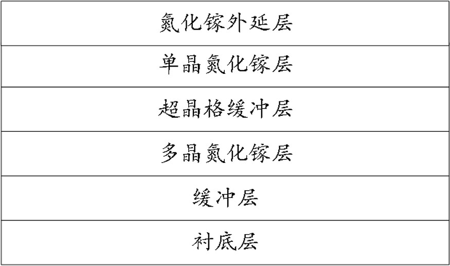
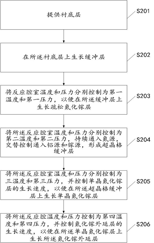
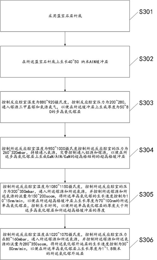
[0044] The core of the present invention is to provide a gallium nitride epitaxial sheet and a growth method of its epitaxial sheet, increasing the polycrystalline nitride layer buffer stress, superlattice buffer layer further buffer stress, improves crystal quality, single crystal gallium gallium Improve the quality of the gallium nitride epitaxial sheet, reduce the dislocation density, and finally form high quality gallium nitride epitaxial sheets.

[0045] In order to better understand the present invention, the present invention will be described in detail below with reference to the accompanying drawings and specific embodiments. Obviously, the described embodiments are merely the embodiments of the invention, not all of the embodiments. Based on the embodiments of the present invention, all other embodiments obtained by those of ordinary skill in the art are in the range of the present invention without making creative labor premise.

[0046] Please refer to figure 1 , figur...


PUM

PropertyMeasurementUnit
thicknessaaaaaaaaaa
thicknessaaaaaaaaaa
thicknessaaaaaaaaaa

Abstract

The invention discloses a gallium nitride epitaxial wafer and a method for growing the epitaxial wafer, comprising: a substrate layer, a buffer layer, a polycrystalline gallium nitride layer, a superlattice buffer layer, a single crystal gallium nitride layer and a gallium nitride layer Epitaxial wafer, using sapphire as the substrate layer, growing a buffer layer on the substrate layer, growing a polycrystalline gallium nitride layer on the buffer layer, growing a superlattice buffer layer on the polycrystalline gallium nitride layer, and growing a superlattice buffer layer on the superlattice buffer layer grow a single crystal gallium nitride layer on the single crystal gallium nitride layer, the thickness of the single crystal gallium nitride layer is greater than the thickness of the polycrystalline gallium nitride layer and the thickness of the superlattice buffer layer, and finally grow the nitride layer on the single crystal gallium nitride layer gallium epitaxial layer. The present invention adopts buffer layer and polycrystalline gallium nitride layer to release the stress from lattice mismatch. The superlattice buffer layer can not only buffer the stress, but also improve the lattice quality. The single crystal gallium nitride layer can mention nitrogen The quality of the gallium nitride epitaxial wafer is reduced, and the dislocation density is reduced, thereby forming a high-quality gallium nitride epitaxial layer.

Description

Technical field [0001] The present invention relates to the field of semiconductor, and more particularly to a gallium nitride epitaxial sheet and a growth method of its epitaxial sheet. Background technique [0002] As the preparation of the gallium nitride epitaxial sheet is mainly carried out from the epitaxial epitaxial growth gallium nitride from sapphire, the conventional buffer layer is formed, and the buffer layer is formed, and the outer sheet and liner can be buffered. The stress between the bottom, but due to the lattice mismatch of the gallium nitride and sapphire substrate, it produces only a layer of buffer layer and cannot completely buffer stress, due to the presence of stress, the epitaxial sheet The song; on the other hand, a single buffer layer Aln or AlGaN is not high, and the structure of the epitaxial sheet is also required to further optimize the structure of the epitaxial sheet to form a high quality epitaxial structure. [0003] In summary, how to generat...

Claims


Application Information

Patent Timeline
Patent Type & Authority Patents(China)
IPC IPC(8): C30B29/68C30B25/18C30B25/20C30B28/14C30B29/40
CPCC30B29/68C30B29/406C30B29/403C30B25/183C30B25/20C30B28/14
Inventor 李利哲王国斌
Owner JIANGSU INST OF ADVANCED SEMICON CO LTD
Why Eureka
Try Eureka