OLED pixel compensation circuit and OLED pixel compensation method

A technology for compensating circuits and pixels, applied in instruments, static indicators, etc., can solve problems such as unevenness, organic light-emitting diode brightness attenuation, brightness difference, etc., achieve uniform panel display, overcome threshold voltage drift, and prolong service life.

Pending Publication Date: 2021-12-31
FUJIAN HUAJIACAI CO LTD
View PDF0 Cites 1 Cited by
  • Summary
  • Abstract
  • Description
  • Claims
  • Application Information

AI Technical Summary

Problems solved by technology

[0004] At present, there are some problems in OLED, for example, due to the influence of low temperature polysilicon (LTPS, Low Temperature Poly-silicon) and metal oxide (Metal Oxide) thin film transistor process, the non-uniformity of the threshold voltage Vth of thin film transistors at different positions, resulting in organic The current difference and brightness difference of light-emitting diodes are perceived by the human eye, that is, the mura phenomenon, and the organic light-emitting diode itself will gradually decay with the increase in brightness between lights.

Method used


Image

  • OLED pixel compensation circuit and OLED pixel compensation method
  • OLED pixel compensation circuit and OLED pixel compensation method
  • OLED pixel compensation circuit and OLED pixel compensation method

Examples


Embodiment Construction

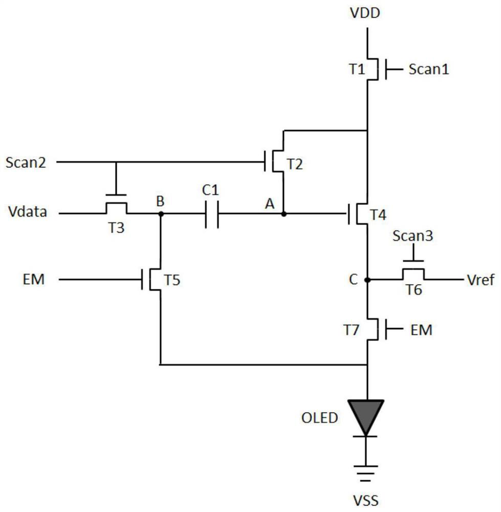
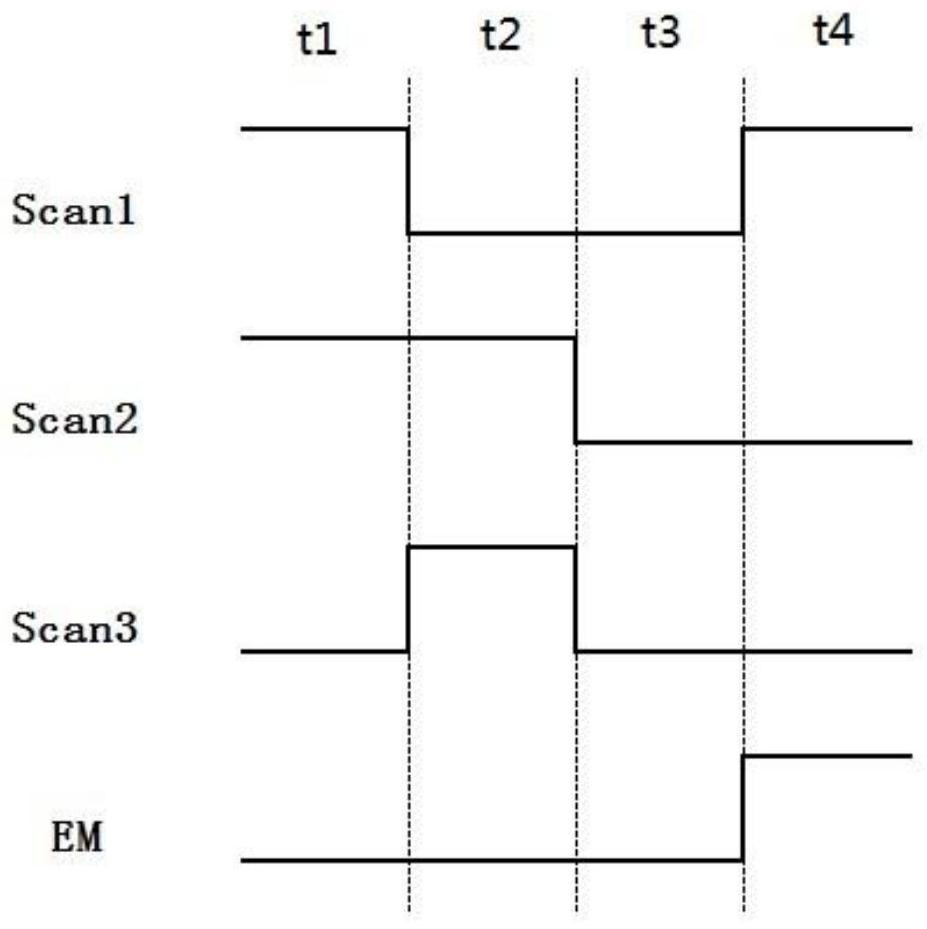
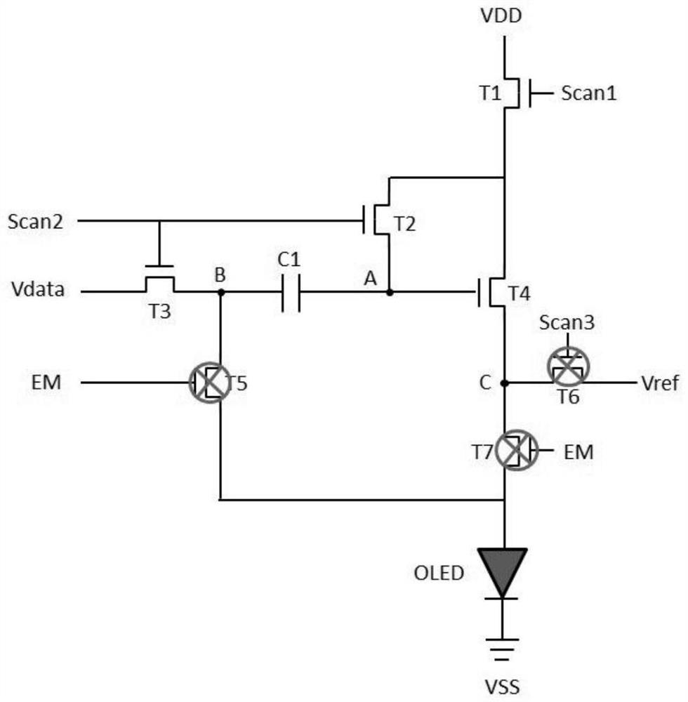
[0031] see figure 1 As shown, the embodiment is an OLED pixel compensation circuit, which includes: a first thin film transistor T1, a second thin film transistor T2, a third thin film transistor T3, a fourth thin film transistor T4, a fifth thin film transistor T5, and a sixth thin film transistor T6 , a seventh thin film transistor T7, an organic light emitting diode OLED and a compensation capacitor C1;

[0032] The drain of the first thin film transistor T1 is connected to the transmission terminal VDD of the DC high voltage power supply, the gate of the first thin film transistor T1 is connected to the first scan signal transmission terminal Scan1, and the sources of the first thin film transistor T1 are respectively connected to the the drain of the second thin film transistor T2 and the drain of the fourth thin film transistor T4;

[0033] The gate of the second thin film transistor T2 is connected to the second scanning signal transmission terminal Scan2, and the sour...


PUM


Abstract

The invention relates to an OLED (Organic Light Emitting Diode) pixel compensation circuit and an OLED pixel compensation method, seven thin film transistors, one compensation capacitor and one organic light emitting diode are adopted to form a 7T1C framework, and the driving time sequence of pixels is sequentially divided into four stages of resetting, compensation, data storage and light emitting. As the seventh thin film transistor is in a closed state in the reset, compensation and data storage stages, the organic light emitting diode does not emit light, and the seventh thin film transistor is in an open state in the light emitting stage, the current flowing through the organic light emitting diode is irrelevant to the threshold voltage and the driving voltage of the organic light emitting diode. By adopting the technical scheme, not only can threshold voltage drift of the driving thin film transistor be effectively compensated, but also brightness change caused by electrical deterioration of the organic light-emitting diode can be compensated, and the display quality of the organic light-emitting diode is improved.

Description

technical field [0001] The invention relates to the field of display technology, in particular to an OLED pixel compensation circuit and an OLED pixel compensation method. Background technique [0002] In recent years, Organic Light-Emitting Diode (OLED) has been widely used in smart on mobile phones, TVs, mobile wearables, and microdisplays. [0003] Generally, the luminance of an organic light-emitting diode is directly proportional to the current, and the current is provided by the driving thin film transistor, which is related to the characteristic parameters of the driving thin film transistor. The formula for driving current of an OLED is: I oled =1 / 2 µ n C ox W / L(Vgs-Vth) 2 ,in µ n is a parameter related to the electron mobility of the driving thin film transistor, C ox , W / L are parameters related to the channel size of the thin film transistor, and Vgs and power supply voltage are related to the driving voltage of the organic light emitting diode. It can ...

Claims


Application Information

Patent Timeline
Patent Type & Authority Applications(China)
IPC IPC(8): G09G3/3208G09G3/3266G09G3/3258
CPCG09G3/3208G09G3/3266G09G3/3258G09G2320/0233
Inventor 钟慧萍郭智宇陈廷安
Owner FUJIAN HUAJIACAI CO LTD
Why Eureka
Try Eureka