Bump connection placement in quantum devices in a flip chip configuration

A flip-chip and bump technology applied in the field of component placement, which can solve the problems of additional complexity and increased execution time of quantum algorithms

Pending Publication Date: 2022-01-07
IBM CORP
View PDF0 Cites 0 Cited by
  • Summary
  • Abstract
  • Description
  • Claims
  • Application Information

AI Technical Summary

Problems solved by technology

Likewise, simply increasing the length of two parallel rows (e.g., using two parallel rows of twelve qubits each) results in quantum devices with undesired additional area and the separation of qubits at one end of the row

Method used


Image

  • Bump connection placement in quantum devices in a flip chip configuration
  • Bump connection placement in quantum devices in a flip chip configuration
  • Bump connection placement in quantum devices in a flip chip configuration

Examples


Embodiment Construction

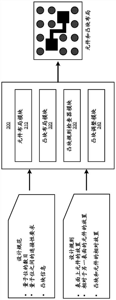
[0029] An internal qubit is a qubit that is not located on the periphery of the qubit configuration in the quantum device; in other words, the qubit is located at a physical location other than the periphery of the qubit configuration in the quantum device. The illustrative embodiments recognize that one solution for accessing internal qubits is to configure the quantum device in a flip-chip configuration. A flip-chip configuration, or simply flip-chip, uses bumps already deposited on one or both surfaces to interconnect one surface of a device or chip with the other surface of a second chip so that the two surfaces are parallel to each other, And the bumps on one surface connect to corresponding bumps or surface locations on the second surface. A bump is a conductive structure formed three-dimensionally on a two-dimensional surface using at least a conductive material and in some cases a superconductive material. One attribute of bumps as contemplated herein is that the bump...


PUM


Abstract

Within a layout of a first surface in a flip chip configuration, a bump restriction area is mapped according to a set of bump placement restrictions, wherein a first bump placement restriction specifies an allowed distance range between a bump and a qubit chip element in a layout of the first surface, and wherein a second bump placement restriction specifies an allowed distance range between the bump and a qubit chip element in a layout of a second surface in the flip chip configuration. An electrically conductive material is deposited outside the bump restriction area, to form the bump, wherein the bump comprises an electrically conductive structure that electrically couples a signal between the first surface and the second surface and is positioned according to the set of bump placement restrictions.

Description

technical field [0001] The present invention generally relates to methods, systems and computer program products for component placement in quantum devices. More specifically, the present invention relates to methods, systems and computer program products for bump connection placement in quantum devices in flip-chip configurations. Background technique [0002] Hereinafter, a "Q" prefix in a word or phrase indicates a reference to that word or phrase in the context of quantum computing, unless clearly distinguished when used. [0003] Molecules and subatomic particles obey the laws of quantum mechanics, the branch of physics that explores how the physical world works at a fundamental level. At this level, particles behave in strange ways, assume more than one state at the same time, and interact with other particles very far away. Quantum computing exploits these quantum phenomena to process information. [0004] The computers we use today are called conventional computer...

Claims


Application Information

Patent Timeline
IPC IPC(8): G06F30/392G06F30/398H01L23/498H01L23/00G06F113/18G06F115/12
CPCG06F30/392G06F30/398H01L23/49838H01L23/49811H01L24/10H01L24/14G06F2113/18G06F2115/12H01L2224/1412G06N10/00G06F30/39G06F30/394G06F30/30G06F2111/14H01L2224/14131H01L2224/14133H01L2224/16145H01L2224/14134H01L24/16H01L2224/14151H01L2224/14154H01L2924/381H01L2924/00012G06F2111/12G06F30/337G06F30/3308G06F30/327H01L24/06H01L2225/06513Y10S977/72Y10S977/839B82Y10/00
Inventor 邵东兵M·布林克
Owner IBM CORP
Why Eureka
Try Eureka