Method for manufacture of nanostructure electrical devices

a technology of electrical devices and nanostructures, which is applied in the direction of superconductor devices, electrical apparatus, semiconductor devices, etc., can solve the problems of affecting the quality of electrical devices, and no known recipe for selective removal of these metals from semiconductors, etc., to reduce the need for post-processing of nanoscale devices, improve and improve the effect of the control of patterned growth

Pending Publication Date: 2022-05-19
UNIVERSITY OF COPENHAGEN
View PDF0 Cites 3 Cited by
  • Summary
  • Abstract
  • Description
  • Claims
  • Application Information

AI Technical Summary

Benefits of technology

[0010]Junctions made using nanowires as both the nanostructure growth object and the shadow structure have been disclosed in WO 2017 / 153388 and in Gazibegovic Nature, 548, 434 (2017). One purpose of the present disclosure is to improve the control of this patterned growth. Another purpose is to reduce the need for post-processing of nanoscale devices.
[0011]In a first aspect the present disclosure therefore relates to a method for manufacturing a substrate for growth of crystalline nanostructures, the method comprising the step of depositing one or more layers of a crystal growth compatible dielectric material, e.g. an epitaxial growth condition compatible dielectric material, such as silicon oxide, in a predefined pattern on the surface of a crystal growth compatible substrate to create a predefined etch pattern of said crystal growth compatible material. Subsequently the substrate surface can be selectively etched around said etch pattern to provide at least one under-etched platform which is vertically raised from the (etched) substrate surface. By having the platform in a chemically stable material, etching can be provided around the shadow structure to create under-etching of the platform such that the platform is vertically displaced but substantially parallel to the substrate surface, which corresponds to the growth plane of the deposition material. The configuration, geometry and location of the platform structure can therefore be very precisely controlled and determined on a nano- and micron-scale.

Problems solved by technology

The requirement for subsequent processing poses several challenges for the approach.
Other relevant superconductors, such as niobium-based alloys, tantalum, vanadium, MgB2, each have superior properties such as higher critical magnetic fields and higher transition temperatures and have crystal structures allowing epitaxial integration with relevant semiconductors, however, no known recipes exist which allow selective removal of these metals from the semiconductors.
As a consequence, these combinations can hardly be explored.
Even in the cases where process recipes do exist, processing of the superconductor will often damage the semiconductor to some degree, possibly degrading device performance and introducing device-to-device variations.
Such serial work where the device is designed around each nanowire is un-scalable and therefore unsuited in large scale applications.

Method used


Image

  • Method for manufacture of nanostructure electrical devices
  • Method for manufacture of nanostructure electrical devices
  • Method for manufacture of nanostructure electrical devices

Examples


example

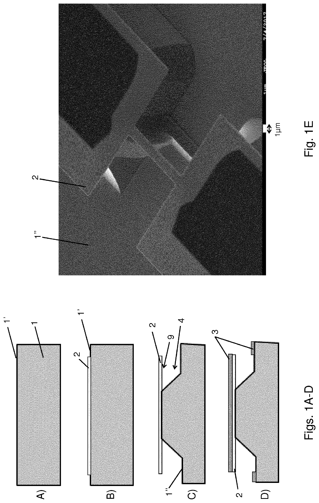
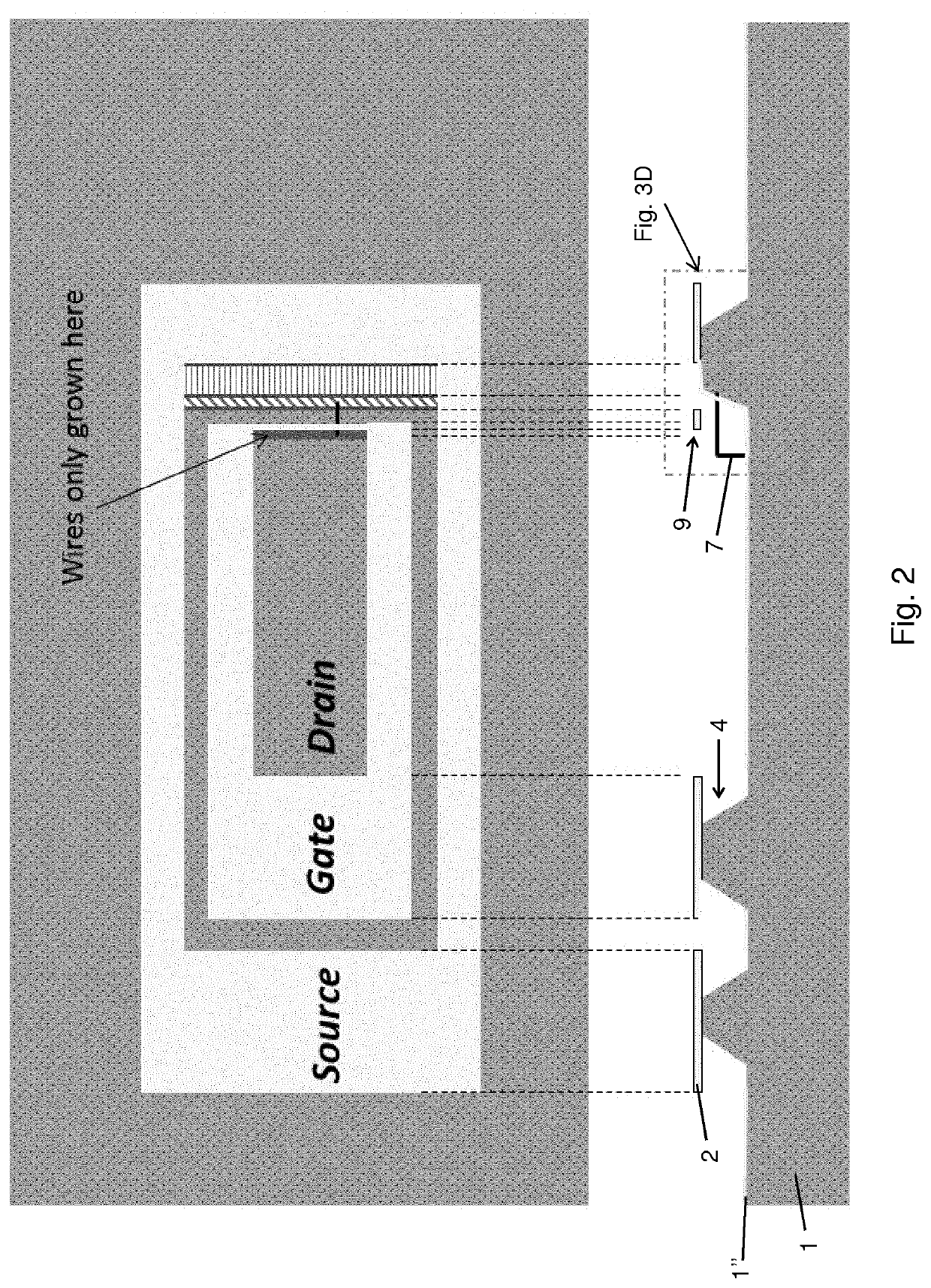
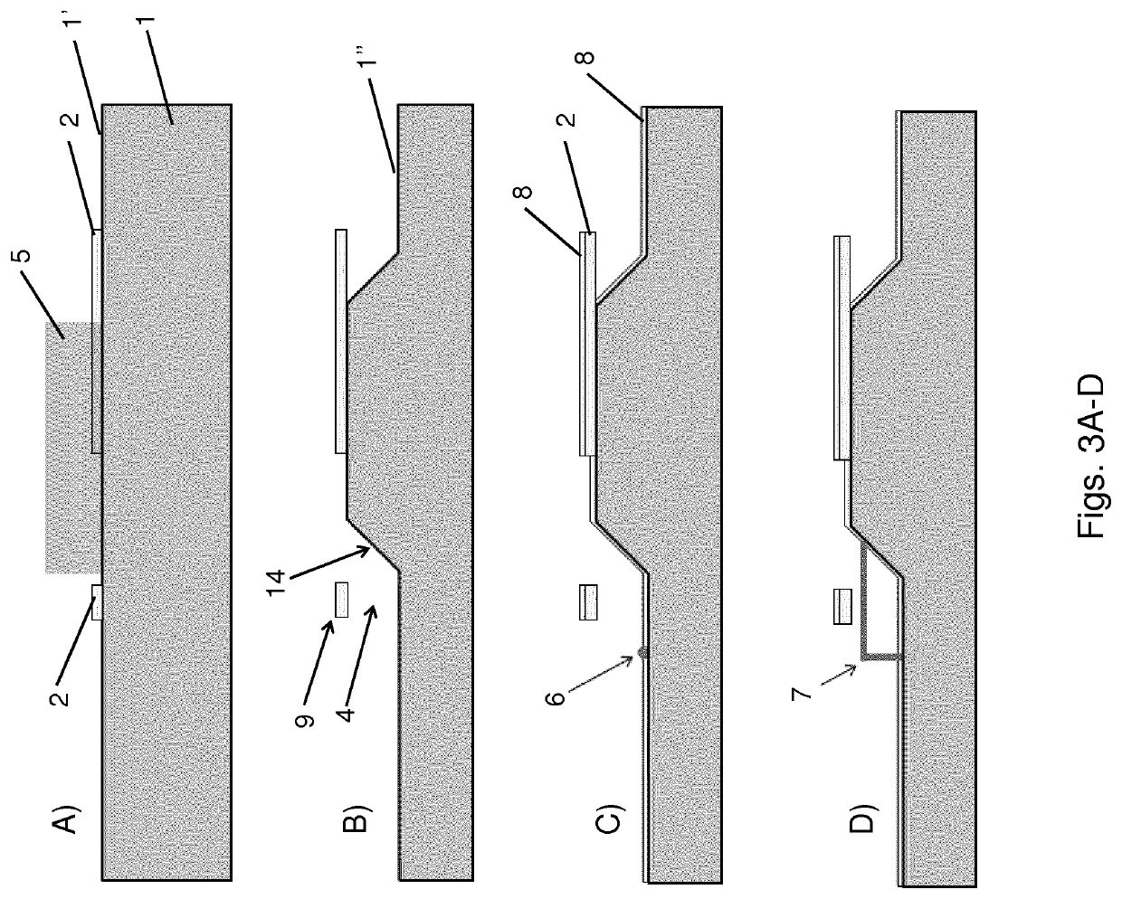
[0120]FIGS. 1A-D show cut-through side views of one example of the presently disclosed approach of vertically displacing a platform from a substrate surface. In FIG. 1A a section of a substrate 1 of epi-ready InAs is shown, the substrate having a substrate surface 1′. In FIG. 1B a platform 2 of SiO has been defined on the substrate surface 1′ using lithography. In FIG. 1C etching has been applied. The platform 2 is untouched by etching but the substrate surface 1′ has been etched leaving the under-etched platform 2 which is vertically displaced from but parallel to the new substrate surface 1″, parts 9 of the platform are suspending the substrate surface 1″ leaving a void 4 below the suspended parts 9. FIG. 1D illustrates the deposition of a metal layer 3 on the platform 2 and the substrate surface 1″. With the metal layer 3 deposited on top of the insulating SiO layer, i.e. the platform 2, and the platform 2 being suspended from the substrate surface 1″, the metal layer 3 on the pl...


PUM

PropertyMeasurementUnit
thicknessaaaaaaaaaa
temperatureaaaaaaaaaa
thicknessaaaaaaaaaa

Abstract

The present disclosure further relates to nanostructures, in particular hybrid nanostructures with patterned growth of various layers for use in nanoscale electronic devices, such as hybrid semiconductor nanostructures with patterned growth and/or deposition of superconducting material for use in quantum devices. The presently disclosed method can be utilized for in-situ manufacturing of nanoscale electronic devices that have not been contaminated by ex-situ processes. One embodiment relates to a method for manufacturing a substrate for growth of crystalline nanostructures, the method comprising the steps of: depositing one or more layers of a crystal growth compatible dielectric material, such as silicon oxide, in a predefined pattern on the surface of a crystal growth compatible substrate to create a predefined etch pattern of said crystal growth compatible material, and selectively etching the substrate surface around said etch pattern to provide at least one under-etched platform which is vertically raised from the etched substrate surface.

Description

[0001]The present disclosure relates to nanostructures, in particular hybrid nanostructures with patterned growth of various layers for use in nanoscale electronic devices, such as hybrid semiconductor nanostructures with patterned growth and / or deposition of superconducting material for use in quantum devices. The presently disclosed method can be utilized for in-situ manufacturing of nanoscale electronic devices that have not been contaminated by ex-situ processes.BACKGROUND OF INVENTION[0002]Hybrid structures between semiconducting nanowires and superconductors are an emerging platform for superconducting electronics, in particular for engineering topologically protected quantum states which can be used as the basic building blocks of a quantum processor. The hybrid structures are also attractive for other superconducting quantum bits, so-called gatemons.[0003]In order for such devices to work, the interface between the semiconductor and superconductor needs to be of high quality...

Claims


Application Information

Patent Timeline
Patent Type & Authority Applications(United States)
IPC IPC(8): H01L29/06H01L39/24
CPCH01L29/068H01L39/2458H01L29/66977H01L39/2496H01L39/2461H01L29/0673H01L29/7613B82Y10/00B82Y40/00H10N60/128H10N60/0604H10N60/0912H10N60/0941H10N60/0632
Inventor JESPERSEN, THOMAS SANDNYGÅRD, JESPERCARRAD, DAMONBJERGFELT, MARTIN
Owner UNIVERSITY OF COPENHAGEN
Why Eureka
Try Eureka