Magnetic track memory
A track memory and magnetic technology, applied in the field of magnetic track memory, can solve the problems of consumption, high energy, increased power consumption, etc., achieve high anisotropy, reduce anisotropy, and reduce write current Effect
- Summary
- Abstract
- Description
- Claims
- Application Information
AI Technical Summary
Problems solved by technology
Method used
Image
Examples
Embodiment 1
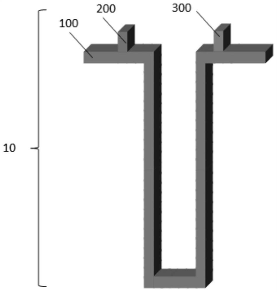
[0046] Example 1: The figure 1 , The magnetic track 10 by the magnetic nanowires memory circuit 100, a write device 200, 300. The reading device. Track magnetic nanowires 100 exhibit "U" shape. Magnetic nanowires 100 may track the magnetization direction perpendicular to the film surface (a film surface herein refers to a magnetic thin film surface), or parallel to the film surface, or forming any angle with the surface of the film. Read device 300 may track the magnetic nanowires 100 constituting a magnetic tunnel junction (MTJ) structure. Wherein magnetic domains in the magnetic nanowires 100 constituting a magnetic circuit electrode "MTJ read", the read device comprising a read MTJ 300 of the tunneling barrier layer and the second magnetic electrode. When the direction of magnetization of the magnetic domains of the magnetic track nanowire 100 changes, the resistance value of the read MTJ is changed, the stored information can be read by a change in the resistance value. Read d...
Embodiment 2
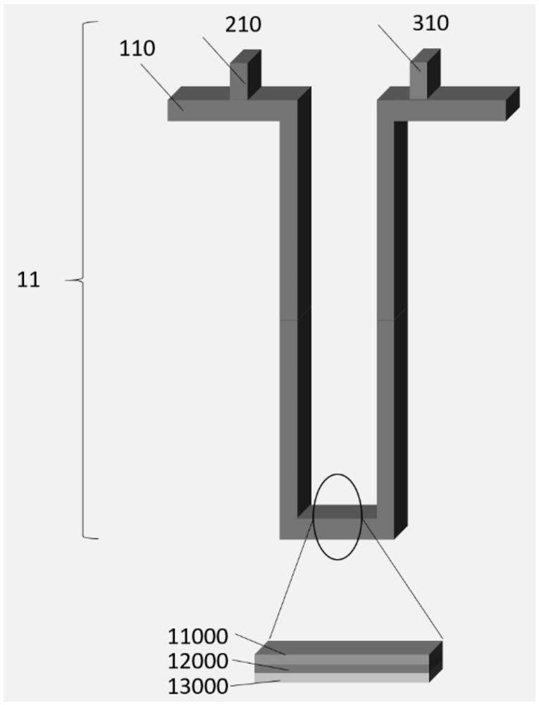
[0048] Example 2: The figure 2 , The magnetic track 11 by the magnetic nanowires memory circuit 110, a write device 210, reading device 310 components. Track magnetic nanowires 110 exhibit "U" shape. The magnetization direction of the magnetic track nanowires 110 may be vertical to the film surface, or parallel to the film surface, or forming any angle with the surface of the film. Track magnetic nanowires comprising a seed layer 110 13,000, a magnetic layer and a cover layer 11,000 12,000 multi-layer material. The magnetic layer may comprise 12,000 multilayered magnetic and non-magnetic thin film. Magnetic thin film can be separated between different non-magnetic film, and there is a mutual exchange coupling. A common exchange coupling is present in the artificial antiferromagnetic (SAF) structure. In this structure, the magnetic thin film adjacent to a non-magnetic exchange coupling film (such as Ru, Ir, Rh, Re, Os, etc.) occur through each other, thereby achieving magnetic thin...
Embodiment 3
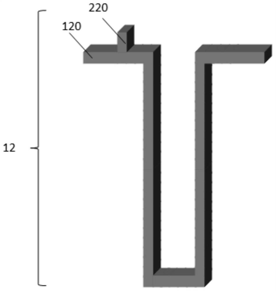
[0049] Example 3: The image 3 , The track 12 by the magnetic nanowires 120, read and write memory device 220 composed of magnetic racetrack. Track magnetic nanowires 120 exhibit "U" shape. Magnetic nanowires 120 may track the magnetization direction perpendicular to the film surface, or parallel to the film surface, or forming any angle with the surface of the film. Device for the reading and writing device with a device, i.e., read and write device 220. Reading and writing device 220 and the track 120 constitute a magnetic nanowires "of the MTJ read" structure. Wherein magnetic domains in the magnetic nanowires 120 constituting a magnetic circuit of the electrode MTJ read, read write device 220 comprises MTJ tunneling barrier layer and the second magnetic electrode. When the direction of magnetization of the magnetic domains of the magnetic track 120 changes nanowires, read MTJ resistance value is changed, the stored information can be read by a change in the resistance value. Wh...
PUM
 Abstract
Description
Claims
Application Information


