Sintering positioning jig for SMD (Surface Mount Device) diode frame

A technology for positioning fixtures and diodes, which is applied in the direction of electrical components, semiconductor/solid-state device manufacturing, circuits, etc., can solve problems that affect the pass rate of SMD diodes, and achieve the effect of ensuring stability and good functionality

Pending Publication Date: 2022-01-11
江苏正芯电子科技有限公司
View PDF0 Cites 0 Cited by
  • Summary
  • Abstract
  • Description
  • Claims
  • Application Information

AI Technical Summary

Problems solved by technology

[0011] The purpose of the present invention is to provide a sintering positioning fixture for a chip diode frame to solve the problem that the positioning fixture in the prior art will seriously affect the qualification rate of the chip diode due to thermal expansion

Method used


Image

  • Sintering positioning jig for SMD (Surface Mount Device) diode frame
  • Sintering positioning jig for SMD (Surface Mount Device) diode frame
  • Sintering positioning jig for SMD (Surface Mount Device) diode frame

Examples


Embodiment 1

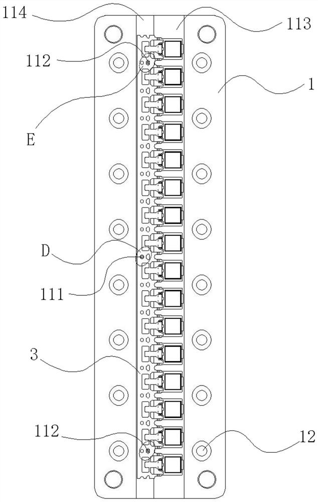
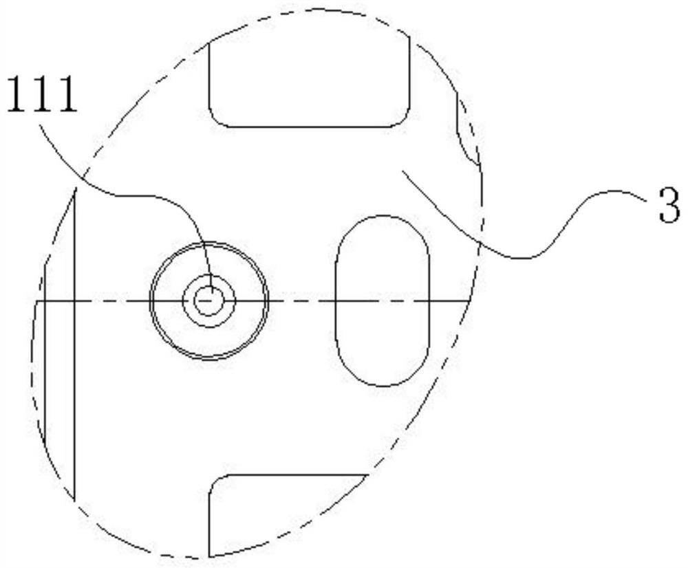
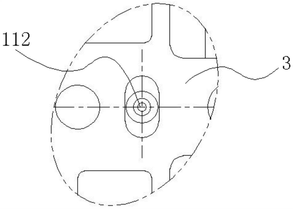
[0040]This embodiment provides a sintering positioning fixture for a chip diode frame, which includes a carrier plate 1, the carrier plate 1 is rectangular, and the upper end surface of the carrier plate 1 is provided with a storage slot 11, and the storage slot 11 is connected with the chip diode frame. 3 Adaptation, the bottom of the storage channel 11 is vertically provided with a positioning pin 111 and a guide pin 112. The storage channel 11 is composed of a placement slot 113 and a positioning slot 114 that are placed side by side, and the depth of the placement slot 113 is greater than that of the positioning slot. 114 depth, the SMD diode frame 3 can be placed stably after being bent and formed; the positioning groove 114 is provided with a relief hole 1141 matched with the cover plate positioning pin 21, and the diameter of the relief hole 1141 is not smaller than the cover plate positioning Twice the diameter of the pin 21, it can position the jig and the SMD diode fr...

Embodiment 2

[0042] This embodiment provides a sintering and positioning fixture for a chip diode frame, which includes a carrier plate 1, the carrier plate 1 is rectangular, and the upper end surface of the carrier plate 1 is provided with a storage slot 11, and the storage slot 11 is made of parallel stickers. The tight placement groove 113 and the positioning groove 114 are formed. The depth of the placement groove 113 is greater than the depth of the positioning groove 114, so that the SMD diode frame 3 can be placed stably after being bent and formed. The bottom of the storage slot 11 is vertically provided with a positioning pin 111 And the guide pin 112, the positioning pin 111 is arranged in the positioning groove 114, which is convenient to adapt to the position of the circular positioning hole on the SMD diode frame, the described guiding pin 112 is arranged in the positioning groove 114, and the guiding pin 112 There are two, which are respectively matched with the oval guide hol...


PUM

PropertyMeasurementUnit
Diameteraaaaaaaaaa
Diameteraaaaaaaaaa

Abstract

The invention discloses a sintering and positioning jigfor an SMD (Surface Mount Device) diode frame. The jig comprises a carrying disc, an object placing through groove is formed in the upper end face of the carrying disc, a positioning pin and a guide pin are vertically arranged at the groove bottom of the object placing through groove, the carrying disc is provided with a plurality of cover plate supporting column receding holes, and at least two mutually independent cover plates are separately arranged above the object placing through groove, each cover plate is provided with a cover plate positioning pin protruding out of the lower end face of the cover plate, the cover plate is provided with a cover plate supporting column protruding out of the lower end face of the cover plate, the cover plate supporting column is matched with the cover plate supporting column receding hole for use, and the cover plate is provided with a guide pin receding through hole matched with the guide pin for use. Through the separated cover plates, when the patch diode frame expands due to high-temperature sintering, the cover plate can transversely move along with the expansion of the patch diode frame under precise cooperation of the cover plate positioning pins and the patch diode frame positioning holes, therefore, the problem that the qualified rate of the SMD diode is seriously affected due to inconsistent thermal expansion rates of the sintering positioning jig and the SMD diode frame is solved.

Description

technical field [0001] The invention belongs to the field of chip diode manufacturing, in particular to a sintering positioning jig for a chip diode frame. Background technique [0002] Due to its simple structure and high reliability, SMD diodes are widely used in important fields such as on-board electronic equipment and safety driving systems of fuel vehicles and new energy vehicles. In order to meet the development requirements of continuously improving automobile quality and safety, various car manufacturers have put forward higher requirements for the dimensional accuracy and reliability of automotive SMD diodes. [0003] At present, the process of sintering the SMD diode frame for automobiles is as follows: [0004] The first step is to place the diode frame on the carrier plate for positioning, place the positioning cover on the lead frame, spot solder paste on the lead frame substrate, assemble the chip, spot solder paste on the chip, spot solder paste on the pins,...

Claims


Application Information

Patent Timeline
IPC IPC(8): H01L21/68
CPCH01L21/68
Inventor 黄永
Owner 江苏正芯电子科技有限公司
Why Eureka
Try Eureka