Integrated circuit test seat and its test interface

A technology for testing interfaces and integrated circuits, which is applied to electronic circuit testing, components of electrical measuring instruments, and electrical measurement. Low, simple structure effect

Active Publication Date: 2008-08-13
ADVANCED SEMICON ENG INC
View PDF0 Cites 0 Cited by
  • Summary
  • Abstract
  • Description
  • Claims
  • Application Information

AI Technical Summary

Problems solved by technology

[0005] But, when adopting aforementioned elastic metal probe as test interface to be used for testing IC package, because the head end of probe head 50 has considerable sharpness, although the spring that is located in main body 51 can provide elasticity to avoid probe The tip 50 touches the surface of the contact (solder ball or pin) provided on the bottom of the IC package under test hard, but it is still easy to puncture the surface of the solder ball or pin due to the sharpness of the probe head 50, thereby The IC package after the test will produce empty welding, cold welding and other phenomena that reduce the qualified rate in the subsequent manufacturing process, and even cause the short circuit of the integrated circuit in severe cases. This is an important shortcoming.
[0006] In addition, as shown in Figure 1, the structure of the existing elastic metal probe 5 is elongated, in order to adapt to this shape, the overall height of the test seat is relatively large
When the IC package under test is placed on the test socket for testing, because the overall height of the test socket is large, the signal of the IC package under test is likely to generate noise due to external interference factors when it is guided to the test machine. , signal attenuation, or electromagnetic interference, resulting in an error in the measured value of the IC package, which is another shortcoming
[0007] In addition, with the densification of IC package contacts, the elastic metal probes produced are becoming finer and finer, and the density of the metal probes needs to be relatively increased, which makes it difficult to manufacture the probes and the cost is relatively expensive, and these probes The needle is fragile and easy to bend and break
Correspondingly, the diameter and pitch of the through-holes of the test socket for accommodating these metal probes are also reduced, and the depth of the through-holes is relatively deep in order to adapt to the elongated shape of the metal probes, making the processing of the test socket very difficult
Therefore, the existing elastic metal probe test interface and its test socket have its own advantages due to the difficulty of processing the through holes of the metal probe and the test socket under the situation that the pitch of the IC package contacts under test is decreasing day by day. limitations, which is another shortcoming of its
[0008] Therefore, there is great inconvenience in the use of the existing elastic metal probe test interface and its IC test seat, so it is extremely necessary to design an innovative IC test interface and its test seat to overcome the above-mentioned shortcomings in the prior art

Method used


Image

  • Integrated circuit test seat and its test interface
  • Integrated circuit test seat and its test interface
  • Integrated circuit test seat and its test interface

Examples


Embodiment Construction

[0022] Relevant detailed description and technical contents of the present invention are as follows now in conjunction with the accompanying drawings:

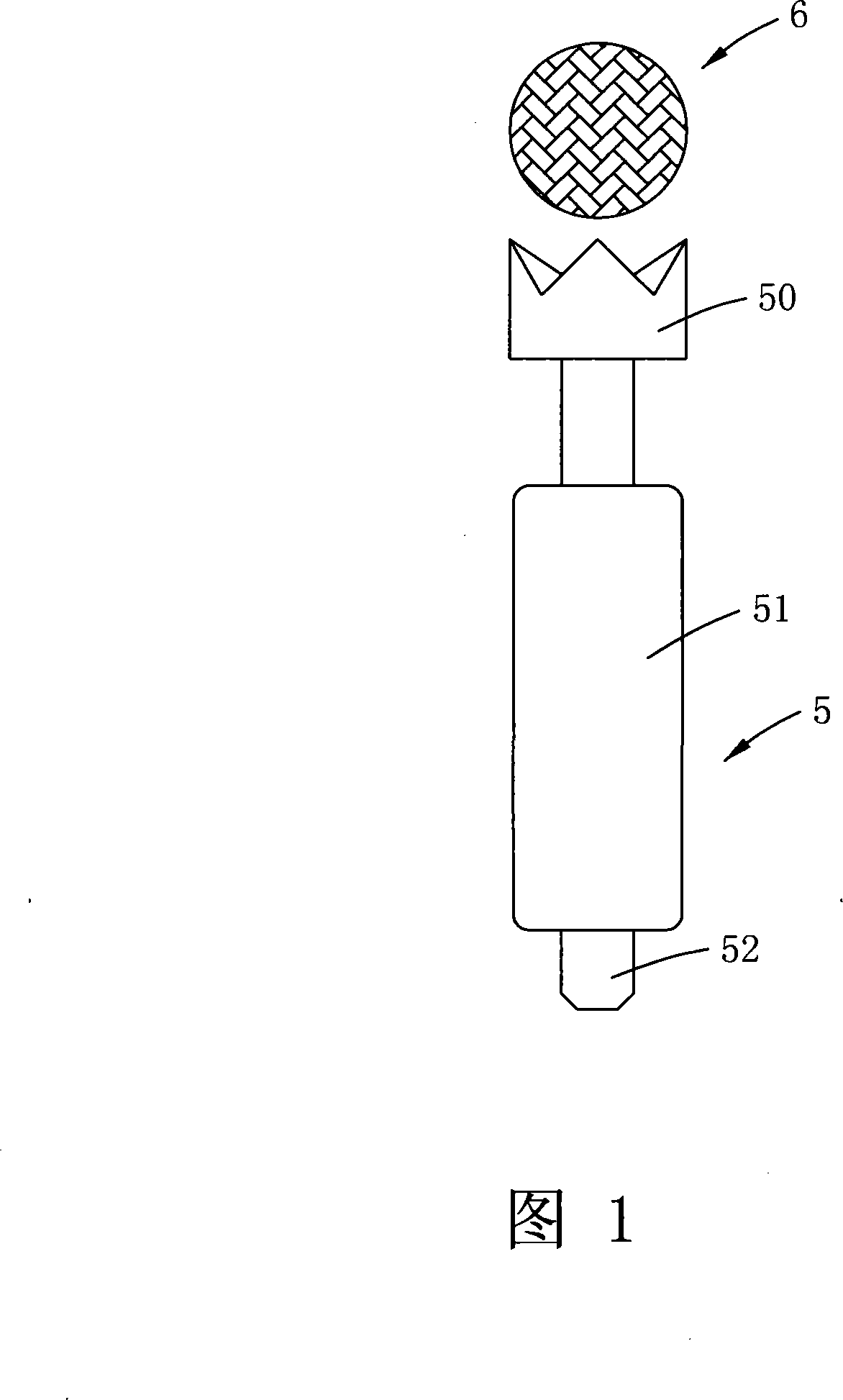
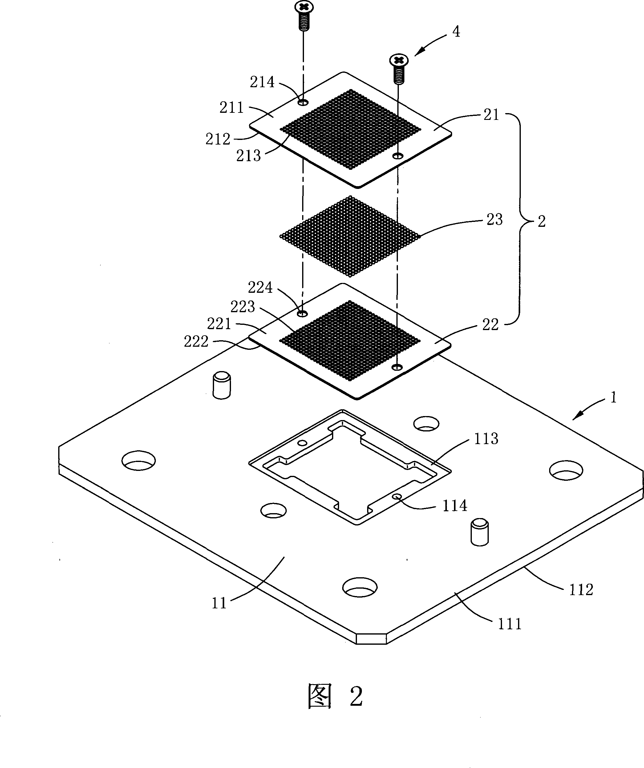
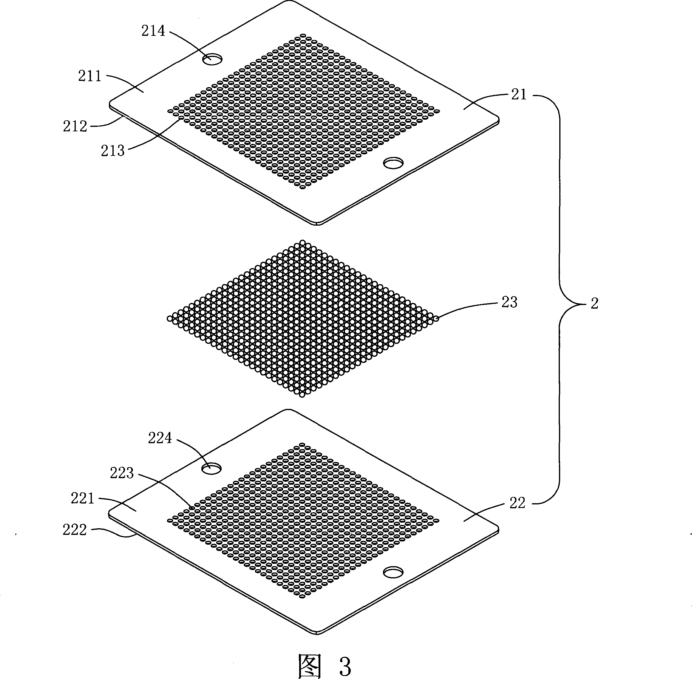
[0023] Please refer to FIG. 2 and FIG. 3 , wherein FIG. 2 is a three-dimensional exploded schematic view of the integrated circuit (IC) test socket 1 of the present invention, and FIG. 3 is a schematic exploded structure schematic diagram of the IC test interface 2 of the IC test socket 1 of the present invention. The test socket 1 is disposed between an IC package to be tested (refer to the IC package 3 shown in FIG. 5 ) and a test board (not shown), and is used for electrical testing of the IC package. The IC test socket 1 includes a test socket body 11 having a top surface 111 , a bottom surface 112 and an opening 113 passing through the top surface 111 and the bottom surface 112 . Two positioning holes 114 are defined at two opposite inner edges of the opening 113 .

[0024] The IC test interface 2 is disposed in the open...


PUM


Abstract

The present invention provides an IC testing seat and testing interface thereof. The IC testing seat comprises of a testing seat body, a top surface, a bottom surface and a hatch through the top and bottom surface. The testing interface is set in the testing seat body which comprises of first and second non-electric conductivity flexible sheet space and many conductive spheres. The first, second non-electric conductivity flexible sheet space has one top surface and bottom surface respectively and many first, second via holes corresponding to meeting points on bottom of IC encapsulation parts. The first, second via holes have identical number and vertical contraposition through combination of first, second non-electric conductivity flexible sheet space and conductive spheres can accepted and fixed in it, and one end of each conductive sphere extends outside the top surface of testing seat body to contact electrically with corresponding meeting points on bottom of IC encapsulation parts, the other end extends outside of the bottom of testing seat body to contact electrically with corresponding meeting points on testing board.

Description

technical field [0001] The invention relates to the field of integrated circuit (IC) testing, in particular to an integrated circuit (IC) test socket for testing IC packages and a test interface thereof. Background technique [0002] After the integrated circuit package (IC Package) is completed, the IC package must undergo a sampling test before leaving the factory to confirm that its design function has indeed met the relevant requirements. Generally, IC packaging testing needs to be tested by means of a combination of three main components. [0003] Firstly, the test handler (Test Handler) of a handling system takes out the packaged IC package from the carrier (Carrier), and installs the IC package on the test socket (Test Socket) matching its bottom contact, and sets Set the environment parameters. Then, the test socket is bonded with the load board, which is a conversion interface for signal transmission contacts, and can connect the signals on the contacts of the IC ...

Claims


Application Information

Patent Timeline
Patent Type & Authority Applications(China)
IPC IPC(8): G01R1/02G01R1/06G01R1/073G01R31/28
Inventor 蔡曜鸿庄庆文张修明
Owner ADVANCED SEMICON ENG INC
Why Eureka
Try Eureka