Novel chip carrying and testing equipment and working method thereof

A technology for testing equipment and chips, which is applied in the direction of optical testing flaws/defects, measuring devices, transportation and packaging, etc. It can solve the problems of no bottom visual correction of chips, inaccurate placement of chips, and no height measurement of chips, etc., to improve handling The effect of quality and test accuracy, avoiding inaccurate picking and placing, and avoiding distance errors

Pending Publication Date: 2022-01-18
上海梓一测控技术有限公司
View PDF0 Cites 0 Cited by
  • Summary
  • Abstract
  • Description
  • Claims
  • Application Information

AI Technical Summary

Problems solved by technology

[0003] The existing chip handling and testing equipment, when in use, does not take a visual photo of the chip, and there is no visual correction position for the bottom of the chip, and there is no visual photo position for the discharge, which leads to inaccurate handling and placement of the chip, and it is easy to overlap after placement At the same time, the existing similar equipment does not measure the height of the chip, and the distance of the suction head cannot be changed, and the test part of the chip handling test equipment usually uses 4 or 32 acupoints to test at the same time, the work efficiency is low, and the matching effect is poor.

Method used


Image

  • Novel chip carrying and testing equipment and working method thereof
  • Novel chip carrying and testing equipment and working method thereof
  • Novel chip carrying and testing equipment and working method thereof

Examples


Embodiment Construction

[0056] The following will clearly and completely describe the technical solutions in the embodiments of the present invention with reference to the accompanying drawings in the embodiments of the present invention. Obviously, the described embodiments are only some, not all, embodiments of the present invention. Based on the embodiments of the present invention, all other embodiments obtained by persons of ordinary skill in the art without making creative efforts belong to the protection scope of the present invention.

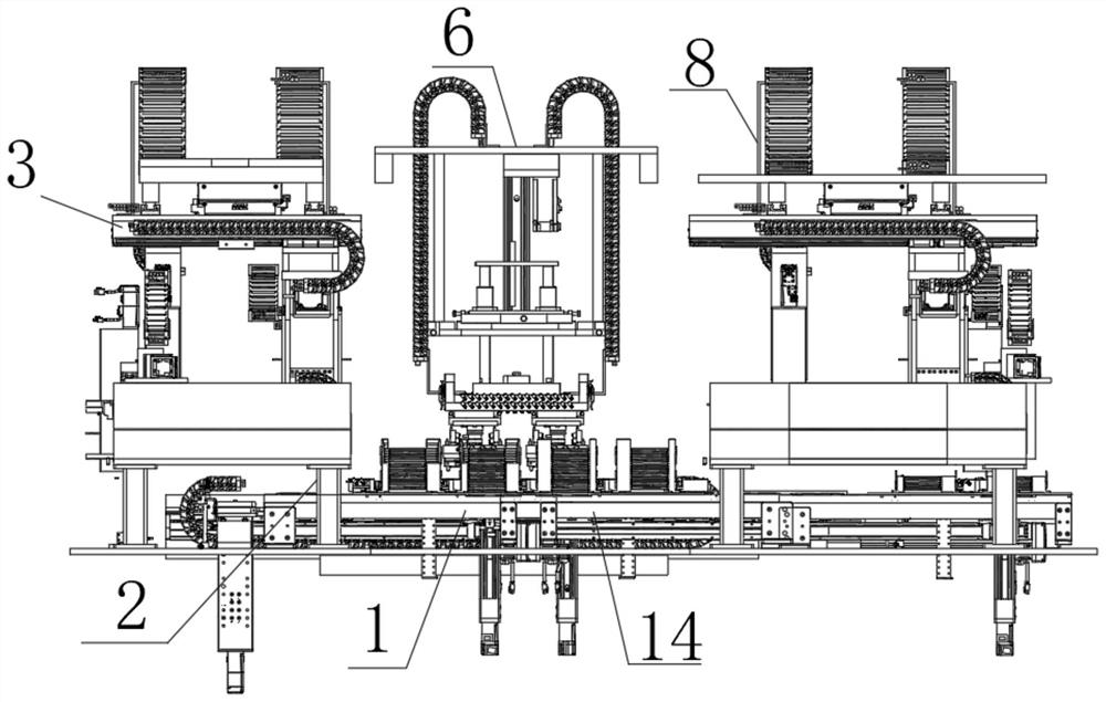
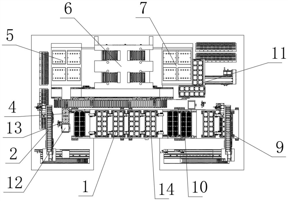
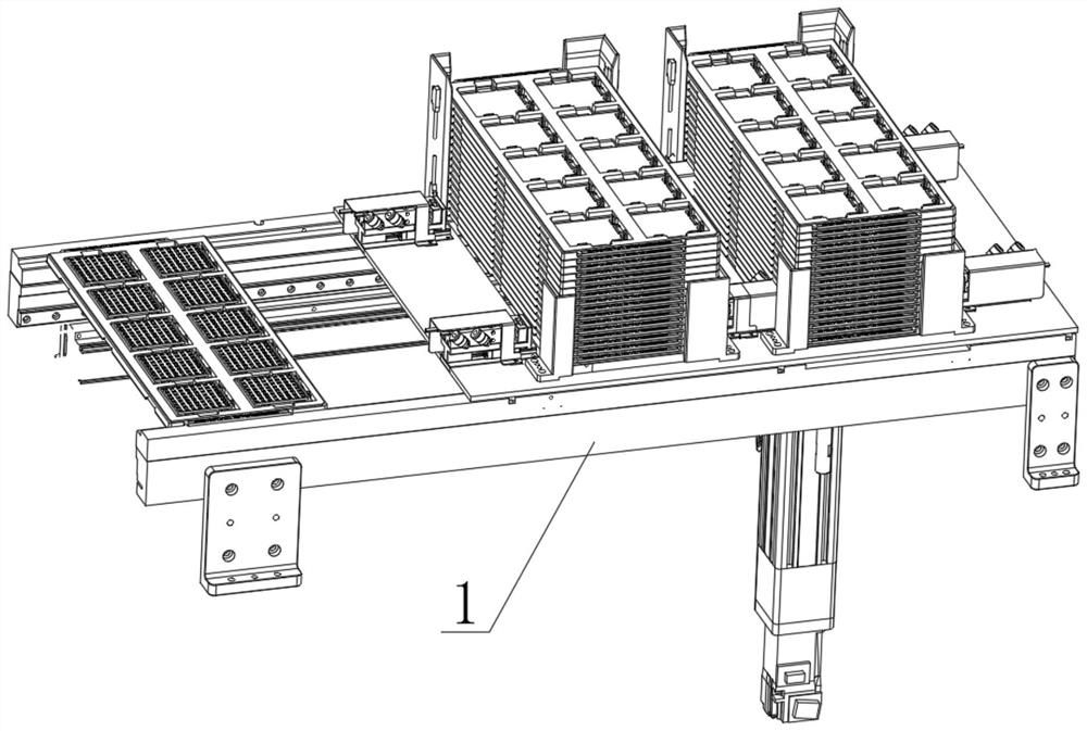
[0057] see Figure 1-Figure 18 , a new type of chip handling and testing equipment, including tray stacking rack 1, loading tray photo height measuring component 2, support plate 201, first camera 202, first light source 203, first movable rod 204, second movable rod 205, height measurement laser sensor 206, feeding suction and handling assembly 3, stand 301, first photographing chamber 302, feeding suction nozzle 303, bottom correction assembly 4, side plate ...


PUM


Abstract

The invention relates to the technical field of chip carrying, and discloses novel chip carrying test equipment and a working method thereof. The novel chip carrying test equipment comprises a tray stacking and feeding frame, a feeding tray photographing and height measuring assembly is installed on the outer side of the tray stacking and feeding frame, a feeding suction and carrying assembly is arranged at the top of the feeding tray photographing and height measuring assembly, a bottom correcting assembly is installed between the tray stacking feeding frame and the feeding tray photographing and height measuring assembly, and a feeding moving assembly is installed on the rear end face of the tray stacking feeding frame. Through the arrangement of the feeding tray photographing and height measuring assembly, feeding suction of a chip is subjected to visual photographing, the suction center position of the chip is given, after suction, the angle of the chip is corrected through a CCD correction camera at the bottom, finally, the chip is placed at the acupuncture point position of a carrier through CCD visual photographing, and after data calculation, the sucked chip can be accurately placed on a set position of the carrier or the tray, so that the problem of inaccurate placement of the chip is effectively solved.

Description

technical field [0001] The invention relates to the technical field of chip handling, in particular to novel chip handling and testing equipment and working methods. Background technique [0002] The technical level of chip handling and testing equipment is an important symbol of the progress of integrated circuit handling and testing technology. Chip testing equipment manufacturers that affect the entire process of integrated circuit production are also one of the important components of the industrial chain. Chip handling and testing equipment is mainly used for automatic loading of chips , then to the suction and transportation of the chip, and then to the test after the placement of the chip. After the test is completed, the suction and transportation go to the receiving, and the receiving is divided into OK products and NG defective products. [0003] The existing chip handling and testing equipment, when in use, does not take a visual photo of the chip, and there is no...

Claims


Application Information

Patent Timeline
Patent Type & Authority Applications(China)
IPC IPC(8): G01N21/89G01B11/06B07C5/00B07C5/02B07C5/36B65G47/90B65G47/52
CPCG01N21/89G01B11/0608B07C5/00B07C5/02B07C5/362B65G47/90B65G47/52
Inventor 邓天桥王焕龙张学东毕爱荣韩禄丰周少峰赵婉婉
Owner 上海梓一测控技术有限公司
Why Eureka
Try Eureka