Integrated miniature LED chip and manufacturing method thereof

An LED chip and integrated technology, applied in electrical components, electric solid devices, circuits, etc., can solve the problems of lower packaging yield and packaging reliability, low packaging-level process requirements and precision, and small size of three-color LED chips. , to achieve the effects of improving packaging yield and packaging reliability, flexible layout and structural design, and flexible structural design

Pending Publication Date: 2022-01-18
FOSHAN NATIONSTAR SEMICON
View PDF0 Cites 1 Cited by
  • Summary
  • Abstract
  • Description
  • Claims
  • Application Information

AI Technical Summary

Problems solved by technology

[0003] At present, the three-color LEDs of the RGB-LED display are separated independently before packaging, and they need to be transferred to the packaging substrate through a large amount of R, G, and B three-color LEDs in sequence, so as to realize the uniform mixing of the RGB three-color LEDs, and the huge The method of mass transfer has problems such as low transfer yield, high transfer accuracy requirements, and low transfer process yield. The more times of mass transfer, the lower the transfer yield; the three-color LED chip of RGB-LED display Small size, large quantity, high packaging cost; at the same time, small size leads to less pad area, small welding area, difficulty in evenly injecting an appropriate amount of soldering material into the welding area, low packaging level process requirements and precision, resulting in poor soldering during packaging and die bonding , there are often abnormalities such as crystal slipping, crystal running, and crystal rotation, which greatly reduce the packaging yield and packaging reliability, thereby further increasing the overall processing cost; There is no light-absorbing medium between adjacent LEDs, resulting in inconspicuous contrast between the non-luminous area (dark area) between adjacent LEDs and the bright area of ​​the LED, resulting in low contrast, low black ratio, and low black ratio on the RGB-LED display. Defects such as weak gray scale and narrow color gamut

Method used


Image

  • Integrated miniature LED chip and manufacturing method thereof
  • Integrated miniature LED chip and manufacturing method thereof
  • Integrated miniature LED chip and manufacturing method thereof

Examples


Embodiment Construction

[0043] In order to make the object, technical solution and advantages of the present invention clearer, the present invention will be further described in detail below in conjunction with the accompanying drawings.

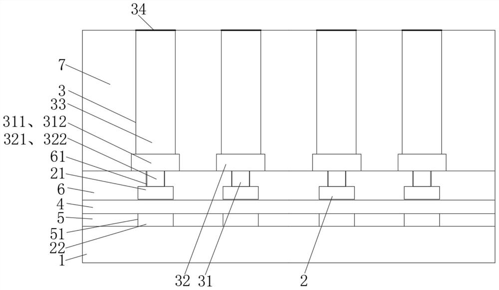
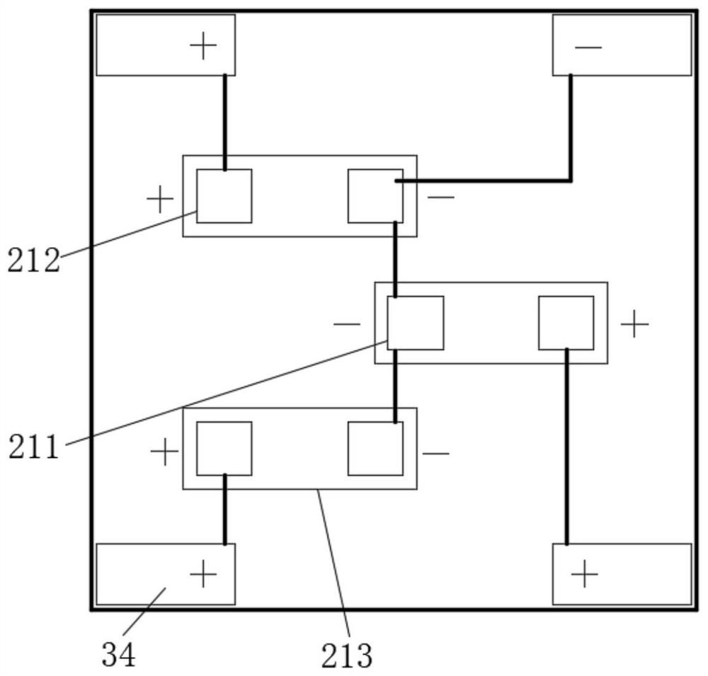
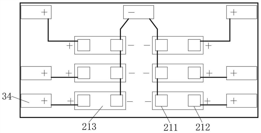
[0044] see figure 1 and figure 2 An integrated micro-LED chip provided by the present invention includes a substrate 1, a light emitting layer 2, a metal connection layer 3 and an encapsulation layer 7. The light emitting layer 2 includes a quantum dot layer 22 and a light emitting element 21. The light emitting layer 2 Can emit the required light color, the metal connection layer 3 is used to form an electrical circuit for the light-emitting element 21, the metal connection layer 3 includes a solder point layer 31, and the light-emitting element 21 includes a first electrode 211 and a second electrode 211. Two electrodes 212 . The encapsulation layer 7 covers the surface of the integrated micro LED chip, thereby fixing the entire integrated micro LED chip.

...


PUM

PropertyMeasurementUnit
sizeaaaaaaaaaa

Abstract

The invention discloses an integrated miniature LED chip and a manufacturing method thereof. The integrated miniature LED chip comprises a substrate, a light emitting layer, a metal connecting layer and a packaging layer, wherein the light emitting layer comprises a quantum dot layer and light emitting pieces, the metal connecting layer comprises a welding spot layer, each light emitting piece comprises a first electrode and a second electrode, the quantum dot layer is arranged corresponding to the light emitting pieces, the welding spot layer comprises a first welding spot area and a second welding spot area, the first welding spot area is electrically connected with the first electrodes in all the light-emitting pieces, and the second welding spot area is electrically connected with the second electrode in the single light-emitting piece. The integrated miniature LED chip can be directly packaged on a circuit board, a packaging process is not needed, the overall processing cost is low, and meanwhile, the problems of crystal slippage, crystal runout, crystal transformation and the like of a Micro LED in a traditional crystal fixing process can be solved; and the contrast between a bright area and a dark area can be highlighted, the black ratio and sharpness are improved, and meanwhile, the transfer efficiency and yield of mass transfer are improved.

Description

technical field [0001] The invention relates to the technical field of semiconductor devices, in particular to an integrated micro LED chip and a manufacturing method thereof. Background technique [0002] LED has a series of advantages such as energy saving, environmental protection, earthquake resistance and safety, and is widely used in lighting, display and other fields. As a high-tech product, LED display has attracted people's attention. The intelligent full-color display screen that adopts computer control and integrates light and electricity has been widely used in advertising media, entertainment culture, traffic guidance, sports and other fields. Its pixels are illuminated by red, green and blue LEDs. Diodes are arranged in a dot matrix to achieve full-color display. As the application of LED display screens in the display field becomes more and more popular, the red, green and blue LED chips and the spacing between the chips also need to be continuously reduced....

Claims


Application Information

Patent Timeline
Patent Type & Authority Applications(China)
IPC IPC(8): H01L33/36H01L33/38H01L33/44H01L33/50H01L27/15H01L33/00
CPCH01L33/36H01L33/387H01L33/44H01L33/50H01L27/156H01L33/005H01L2933/0016H01L2933/0025H01L2933/0041
Inventor 范凯平徐亮易瀚翔靳彩霞李程李瑞迪黎银英
Owner FOSHAN NATIONSTAR SEMICON
Why Eureka
Try Eureka