Semiconductor device and control method thereof

A technology of semiconductors and devices, which is applied in the field of semiconductor devices and their control, can solve the problems of unstable HVIC work, long recovery time from negative, RS trigger cannot be recorded, etc., and achieve the effect of improving efficiency and stability

Pending Publication Date: 2022-01-18
GUANGDONG HIIC SEMICON LTD
View PDF0 Cites 5 Cited by
  • Summary
  • Abstract
  • Description
  • Claims
  • Application Information

AI Technical Summary

Problems solved by technology

[0004] The technical problem to be solved by the present invention is to provide a semiconductor device and its control method for the above-mentioned defects of the prior art, which adopts a double-pulse trigger circuit to solve the problem that the RS flip-flop cannot record due to the long recovery time of VS from negative The signal sent by the single pulse GEN, HVIC work instability problem, effectively improve the efficiency and stability of HVIC

Method used


Image

  • Semiconductor device and control method thereof
  • Semiconductor device and control method thereof
  • Semiconductor device and control method thereof

Examples


Embodiment Construction

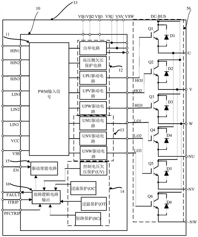
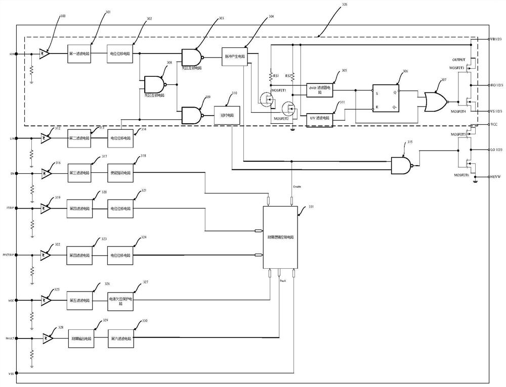
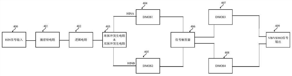
[0021] The specific embodiments of the present invention will be further described below in conjunction with the accompanying drawings. It should be noted here that the descriptions of these embodiments are used to help understand the present invention, but are not intended to limit the present invention. In addition, the technical features involved in the various embodiments of the present invention described below may be combined with each other as long as they do not constitute a conflict with each other.

[0022] In describing the present invention, it should be understood that the terms "center", "longitudinal", "transverse", "length", "width", "thickness", "upper", "lower", "front", " Back", "Left", "Right", "Vertical", "Horizontal", "Top", "Bottom", "Inner", "Outer", "Clockwise", "Counterclockwise", "Axial", The orientation or positional relationship indicated by "radial", "circumferential", etc. is based on the orientation or positional relationship shown in the drawi...


PUM


Abstract

The invention relates to the technical field of electronic circuits, and particularly discloses a semiconductor device and a control method thereof. The semiconductor device comprises an HIVC driving logic circuit, an upper bridge arm driving signal output circuit and a lower bridge arm driving signal output circuit; the upper bridge arm driving signal output circuit and the lower bridge arm driving signal output circuit are both electrically connected with the HIVC driving logic circuit, and the HIVC driving logic circuit comprises a PWM signal cache circuit, an upper bridge arm driving circuit, a lower bridge arm driving circuit and a fault logic control circuit; and the PWM signal cache circuit, the lower bridge arm driving circuit and the fault logic control circuit are electrically connected with the upper bridge arm driving circuit. The double-pulse trigger circuit is adopted, the problems that an RS trigger cannot record a signal sent by a single-pulse GEN due to the fact that the time for VS to recover from the negative state is long, and an HVIC works unstably are solved, and the use efficiency and stability of the HVIC are effectively improved.

Description

technical field [0001] The invention relates to the technical field of electronic circuits, in particular to a semiconductor device and a control method thereof. Background technique [0002] Intelligent Power Module (IPM) is a power drive semiconductor product that combines power electronics and integrated circuit HVIC technology. The power switching device and the high-voltage drive device circuit are integrated together inside, and there are built-in fault detection circuits such as overvoltage, overcurrent, and overheating, which are widely used in inverters, welding machines, servo drives and other systems. The interior is divided into upper bridge arm, lower bridge arm, logic circuit, protection circuit, etc., and the drive control and protection feedback are realized through the logic chip of the integrated circuit. When the intelligent power module is working, on the one hand, it receives the control signal from the MCU to drive the follow-up circuit to work; In ca...

Claims


Application Information

Patent Timeline
Patent Type & Authority Applications(China)
IPC IPC(8): H02M1/088H02H7/12
CPCH02M1/088H02H7/1206
Inventor 冯宇翔张土明潘志坚左安超谢荣才
Owner GUANGDONG HIIC SEMICON LTD
Why Eureka
Try Eureka