Surface micro-crosslinking process suitable for preparing deep-texture film
A technology of micro-crosslinking and deep texture, which is applied in the direction of pretreatment surface, special surface, surface coating liquid device, etc., can solve the problems of incomplete texture transfer, UV resin residue, high cost of mold preparation, etc., and achieve improvement Release effect, control thickness, and avoid the effect of residual glue problem
- Summary
- Abstract
- Description
- Claims
- Application Information
AI Technical Summary
Problems solved by technology
Method used
Image
Examples
Embodiment 1
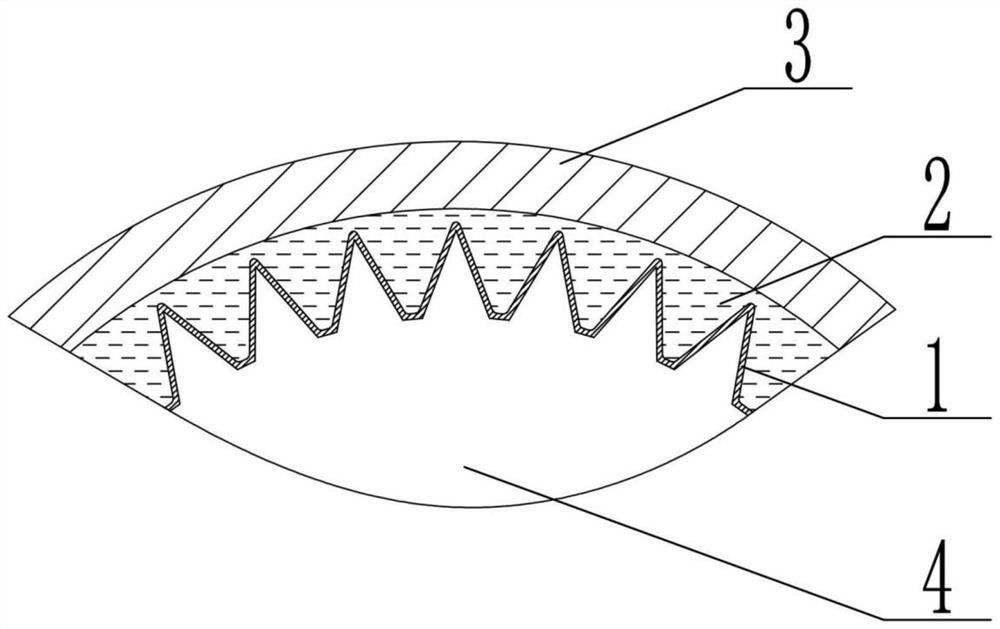
[0057] A surface micro-crosslinking process suitable for preparing deep-textured films, the surface micro-crosslinking process includes a roller mold 4 with a deep texture on the outer surface, and the depth of the deep texture on the roller mold 4 is 10 μm, corresponding to The pitch of adjacent deep textures is 5 μm, and the surface micro-crosslinking process includes the following steps:
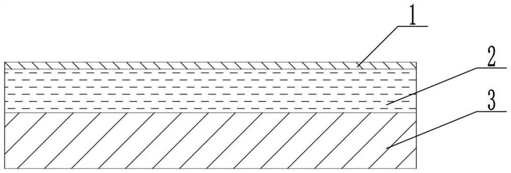
[0058] A, getting thickness is on the PET base film 3 of 30 μ m, and coating one deck UV resin on the upper surface of described PET base film 3, forms UV sol layer 2, and the thickness of described UV sol layer 2 is 15 μ m;
[0059] B. The UV sol layer 2 is radiated and cured at normal temperature and pressure, so that the upper surface of the UV sol layer 2 forms a micro-crosslinked surface 1, and the thickness of the micro-crosslinked surface 1 is 0.05 of the thickness of the UV sol layer 2. times, wherein the degree of micro-crosslinking of the micro-crosslinked surface 1 is controlle...
Embodiment 2
[0078] A surface micro-crosslinking process suitable for preparing deep-textured films, the surface micro-crosslinking process includes a roller mold 4 with a deep texture on the outer surface, and the depth of the deep texture on the roller mold 4 is 20 μm, corresponding to The pitch of adjacent deep textures is 5 μm, and the surface micro-crosslinking process includes the following steps:
[0079] A, getting a thickness on the PET base film 3 of 50 μm, and coating one deck of UV resin on the upper surface of the PET base film 3 to form a UV sol layer 2, the thickness of the UV sol layer 2 is 30 μm;
[0080] B. The UV sol layer 2 is radiated and cured at normal temperature and pressure, so that the upper surface of the UV sol layer 2 forms a micro-crosslinked surface 1, and the thickness of the micro-crosslinked surface 1 is 0.1 of the thickness of the UV sol layer 2. times, wherein the degree of micro-crosslinking of the micro-crosslinked surface 1 is controlled at 8%;
[0...
Embodiment 3
[0098] Preferably, the radiation curing in step B is EB radiation.
[0099] Preferably, the EB radiation is irradiated by an electron beam with 300 MeV, the radiation atmosphere is 95% nitrogen environment, and the radiation time is 1 second.
[0100] Other implementation modes in this embodiment are the same as those in Embodiment 2.
PUM
| Property | Measurement | Unit |
|---|---|---|
| depth | aaaaa | aaaaa |
| thickness | aaaaa | aaaaa |
| thickness | aaaaa | aaaaa |
Abstract
Description
Claims
Application Information


