In-situ PN structure gallium oxide power diode and production method thereof
A technology of power diodes and gallium oxide, applied in semiconductor/solid-state device manufacturing, electrical components, circuits, etc., can solve problems such as large thermal field emission current, improve breakdown voltage, improve interface characteristics, and reduce reverse leakage current Effect
- Summary
- Abstract
- Description
- Claims
- Application Information
AI Technical Summary
Problems solved by technology
Method used
Image


Examples
Embodiment 1
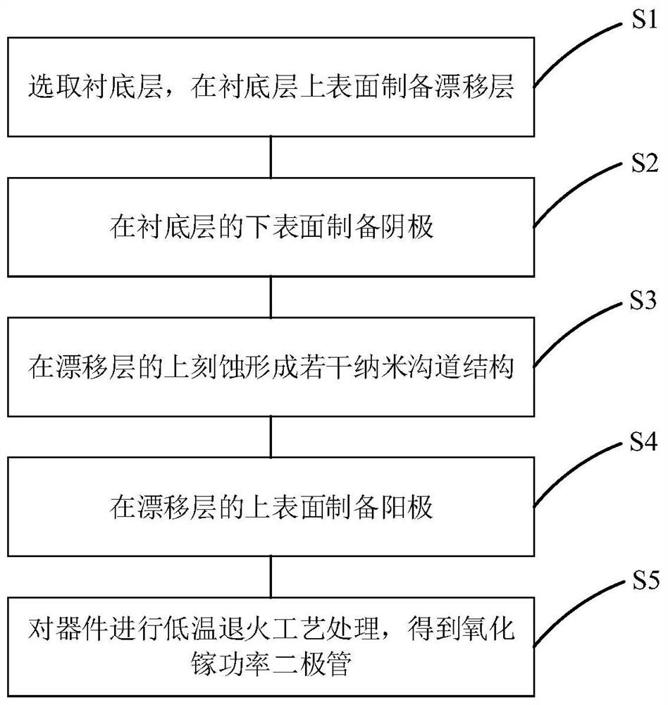
[0037] See figure 1 , figure 1 It is a flowchart of a method for preparing an in-situ PN structure gallium oxide power diode provided by an embodiment of the present invention. As shown in the figure, the method for preparing an in-situ PN structure gallium oxide power diode in this embodiment includes:
[0038] S1: select the substrate layer, and prepare a drift layer on the upper surface of the substrate layer;
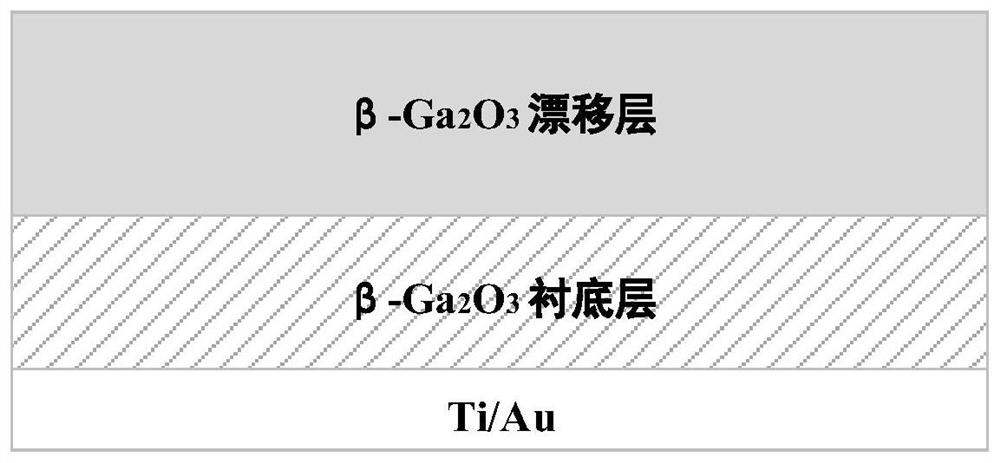
[0039] In this embodiment, optionally, Si or Sn heavily doped β-Ga 2 o 3 As the substrate layer, Si or Sn heavily doped β-Ga 2 o 3 A layer of Si or Sn lightly doped β-Ga is grown on the substrate 2 o 3 as a floating layer.
[0040] In this embodiment, the doping concentration of the drift layer is lower than that of the substrate layer.
[0041] Optionally, the doping concentration of the substrate layer is 5×10 18 cm -3 -5×10 19 cm -3 .
[0042] Optionally, the thickness of the drift layer is 2-14 μm, and the doping concentration is 1×10 15 cm -3 -1×...
Embodiment 2
[0059] See Figure 2a-Figure 2e , Figure 2a-Figure 2e It is a flow chart of the preparation process of an in-situ PN structure gallium oxide power diode provided by the embodiment of the present invention; this embodiment specifically describes the preparation method of the in-situ PN structure gallium oxide power diode in the first embodiment.
[0060] 1. Preparation of gallium oxide power diodes with a drift layer thickness of 2 μm
[0061] Step 1. Select a substrate layer, and prepare a drift layer on the upper surface of the substrate layer.
[0062] Choose heavily Si-doped β-Ga 2 o 3 As the substrate layer, the doping concentration is 5×10 18 cm -3 , in Si heavily doped β-Ga 2 o 3 Above, using the HVPE process, epitaxially grow a layer of Si lightly doped β-Ga 2 o 3 layer as a drift layer, where the thickness of the drift layer is 2 μm, and the doping concentration of the drift layer is 1×10 15 cm -3 ,Such as Figure 2a shown.
[0063] Step 2. Cathode electr...
Embodiment 3
[0094] This embodiment provides an in-situ PN structure gallium oxide power diode, please refer to image 3 , image 3It is a schematic structural diagram of an in-situ PN structure gallium oxide power diode provided by an embodiment of the present invention. As shown in the figure, the bit PN structure gallium oxide power diode of this embodiment includes: a cathode 1, a substrate layer 2, and a drift layer 3 and anode 4. Among them, the cathode 1, the substrate layer 2 and the drift layer 3 are stacked sequentially from bottom to top; the upper surface of the drift layer 3 is etched to form a number of nano-channel structures 301; the anode 4 is arranged on the drift layer 3, and the nano-channel structure The bottom and inner wall of 301; the anode 4 is a Ni / Au metal stack, and the NiO layer 5 with P-type characteristics is formed at the interface between the metal Ni and the drift layer 3, and the NiO layer 5 and the drift layer 3 form a heterogeneous PN junction structur...
PUM
| Property | Measurement | Unit |
|---|---|---|
| Thickness | aaaaa | aaaaa |
| Doping concentration | aaaaa | aaaaa |
| Etching depth | aaaaa | aaaaa |
Abstract
Description
Claims
Application Information
 - Generate Ideas
- Intellectual Property
- Life Sciences
- Materials
- Tech Scout
- Unparalleled Data Quality
- Higher Quality Content
- 60% Fewer Hallucinations
Browse by: Latest US Patents, China's latest patents, Technical Efficacy Thesaurus, Application Domain, Technology Topic, Popular Technical Reports.
© 2025 PatSnap. All rights reserved.Legal|Privacy policy|Modern Slavery Act Transparency Statement|Sitemap|About US| Contact US: help@patsnap.com