A central contact piece, a connector and a crimping end structure of the central contact piece of the connector
A technology of central contacts and connectors, applied in the direction of contact parts, two-part connection devices, connections, etc., can solve problems such as radio frequency transmission failure, substrate damage, etc., and achieve the effects of avoiding excessive stress concentration, reducing pressure, and ensuring integrity
- Summary
- Abstract
- Description
- Claims
- Application Information
AI Technical Summary
Problems solved by technology
Method used
Image
Examples
Embodiment 1
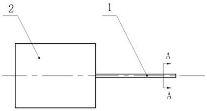
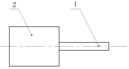
[0073] Such as Figure 8-Figure 10 As shown, this embodiment provides a connector, which includes a connector housing 2 on which a central contact 1 is connected.
[0074] The central contact piece 1 is a strip structure, the central contact piece 1 includes a straight section and an arc section, the straight section and the arc section are integrated, and the straight section and the arc section are smooth In transition, the edges of the ends of the arc segments are rounded, and the ends of the straight segments are fixedly connected to the connector housing 2 .
[0075] The arc section of the central contact 1 under pressure can form a surface contact with the substrate, which is used to disperse the pressure at the crimping part with the substrate, reduce the pressure, and protect the substrate.
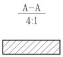
[0076] The cross-section of the central contact is rectangular, the width H of the rectangle is 0.1mm~1mm, the length L is 0.2mm~5mm, the radius R of the arc segment is 0.5mm~10m...
Embodiment 2
[0083] Such as Figure 16-Figure 17 As shown, this embodiment provides a crimping end structure of a central contact of a connector, including the connector described in Embodiment 1 and a high-frequency printed board 3 .
[0084] The connector includes an installation cavity 5 and a connector housing 2, the installation cavity 5 is provided with a connector insulating medium 6, and the connector housing 2 is connected to the installation cavity by connector mounting screws 7 On the body 5, the central contact piece 1 is connected to the connector housing 2.
[0085] The high-frequency printed board 3 is provided with a stripline or a microstrip line 4 .
[0086] Wherein, the central contact 1 is located directly above the stripline or microstrip 4 , and the central contact 1 can form surface contact with the stripline or microstrip 4 under pressure.
[0087] Such as Figure 18-Figure 20 As shown, in this embodiment, the connector housing 2 is an SMP connector housing;
[...
Embodiment 3
[0091] The difference between this embodiment and embodiment 2 is: as Figure 21-Figure 23 As shown, the connector housing 2 is an SMA type connector housing;
[0092] The width H of the cross section of the central contact 1 is 0.35 mm, the length L is 1.2 mm, the radius R of the arc segment is 1.2 mm, and the radius of the edge rounding is 0.1 mm.
[0093] The material of the central contact piece 1 is beryllium bronze, and the coating is nickel-plated on the bottom layer and gold-plated on the surface layer.
PUM
 Abstract
Description
Claims
Application Information


