Method for removing nickel on chemical nickel-plated surface of silicon wafer

A technology of electroless nickel plating and silicon wafers, which is applied in the field of semiconductor silicon wafer production and manufacturing, can solve the problems of large exhaust gas emissions, achieve low cleaning temperature, good cleaning effect, and reduce exhaust gas emissions

Pending Publication Date: 2022-02-11
SHANDONG JINGDAO MICROELECTRONICS
View PDF2 Cites 0 Cited by
  • Summary
  • Abstract
  • Description
  • Claims
  • Application Information

AI Technical Summary

Problems solved by technology

[0004] However, the nitric acid solution at 95°C in this process is easy to form acid mist in the acid tank, such as figure 1 As shown, the amount of exhaust gas is huge, which puts a lot of pressure on the acid mist tower in the subsequent process

Method used


Image

  • Method for removing nickel on chemical nickel-plated surface of silicon wafer
  • Method for removing nickel on chemical nickel-plated surface of silicon wafer

Examples


Embodiment 1

[0016] Prepare raw materials: 37±1% hydrochloric acid, 70±1% nitric acid, pure water, the volume ratio of the three is 8:3:11;

[0017] Device: Heated acid tank with a capacity of 12L with exhaust system.

[0018] Steps: Slowly add 5.5L of pure water to the acid tank;

[0019] Slowly add 4L hydrochloric acid solution into the acid tank to avoid liquid splashing;

[0020] Slowly add 1.5L nitric acid solution into the acid tank to avoid splashing of liquid;

[0021] Turn on the heating switch of the acid tank, raise the temperature to 48°C and keep it;

[0022] Gently put the wafer to be removed from the electroless nickel-plated surface of the silicon wafer into the acid tank to avoid liquid splashing, take it out after 90s and flush it with water, and proceed to the next process.

[0023] After the production of 300 pieces, the waste liquid in the acid tank is collected, used for nickel plating tank cleaning and other operations, and the solution is added to the acid tank a...

Embodiment 2

[0025] This example is basically the same as Example 1, except that the volume ratio of the raw materials 37±1% hydrochloric acid, 70±1% nitric acid, and pure water is 17:6:23, and the cleaning temperature is 46°C.

Embodiment 3

[0027] This example is basically the same as Example 1, except that the volume ratio of the raw materials 37±1% hydrochloric acid, 70±1% nitric acid, and pure water is 3:1:4, and the cleaning temperature is 50°C.

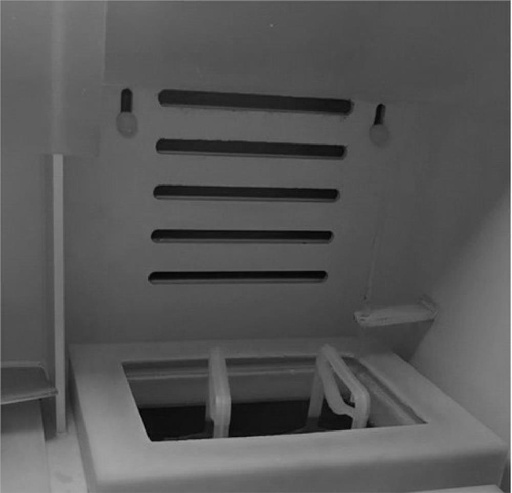
[0028] The results of the above examples show that after 90s, a good cleaning effect is achieved, the nickel layer is uniform, the appearance is good, and there is no obvious acid mist formation, such as figure 2 shown.

[0029] In the above-mentioned embodiments, the solution is replaced after cleaning 300 tablets, and a good cleaning effect can be achieved within 300 tablets.


PUM


Abstract

The invention relates to a method for removing nickel on a chemically nickel-plated surface of a silicon wafer, which belongs to the field of semiconductor silicon wafer production, and the method is characterized by comprising the following steps of: putting a silicon wafer subjected to chemical nickel plating and nickel sintering into mixed acid, and performing cleaning at 46-50 DEG C, the mixed acid being a mixture of a 36-38% hydrochloric acid solution, a 69-71% nitric acid solution and pure water; the mixture of hydrochloric acid, nitric acid and pure water in a specific proportion is used for replacing concentrated nitric acid in the prior art for cleaning chemical nickel plating on the surface of the silicon wafer, the good cleaning effect can be achieved at the temperature of about 48 DEG C, the cleaning time is shortened to 90 s from 120 s in the prior art, the good cleaning effect can be achieved, and the problem of acid mist forming is well solved.

Description

technical field [0001] The invention relates to the technical field of semiconductor silicon chip production and manufacturing, in particular to a method for removing nickel on the surface of silicon chip electroless nickel plating. Background technique [0002] In the field of electronic component manufacturing, silicon wafer is a widely used semiconductor material. During the production of silicon wafers, electroless nickel plating is required on the surface of silicon wafers. Electroless nickel plating is to use divalent nickel ions to react with a reducing agent to form a nickel layer on the surface of the silicon wafer. [0003] In the prior art, most of the electroless nickel plating on silicon wafers adopts the process recorded in the Chinese invention patent with the application number 2018105405765, that is, nickel plating and nickel sintering are carried out in sequence, and then nitric acid is used to clean the surface of silicon wafers. In order to ensure the cl...

Claims


Application Information

Patent Timeline
Patent Type & Authority Applications(China)
IPC IPC(8): C23F1/28
CPCC23F1/28
Inventor 马建建陆新城李智勇江超
Owner SHANDONG JINGDAO MICROELECTRONICS
Why Eureka
Try Eureka