
Parasitic capacitance test structure and method of FinFET

A technology for testing structure and parasitic capacitance, which is applied in semiconductor/solid-state device testing/measurement, circuits, electrical components, etc. It can solve problems such as unfavorable mass production, undetectable M0 parasitic capacitance value, metal gate butterfly depression, etc., to achieve Ease of mass production and calculation

Pending Publication Date: 2022-02-11
SHANGHAI HUALI INTEGRATED CIRCUTE MFG CO LTD
View PDF0 Cites 0 Cited by
  • Summary
  • Abstract
  • Description
  • Claims
  • Application Information

AI Technical Summary

Problems solved by technology

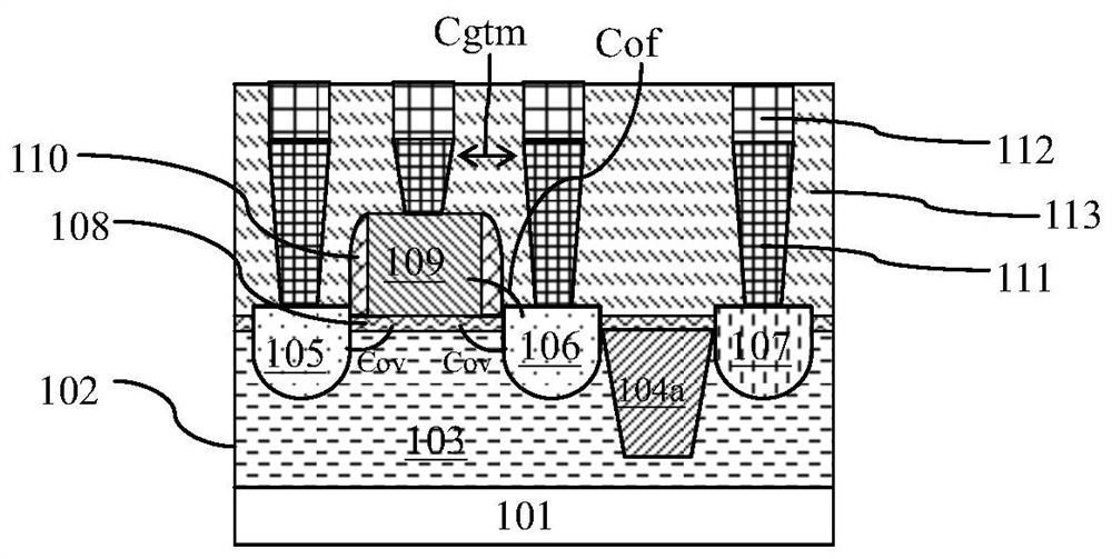
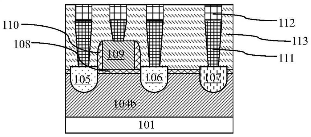
[0012] However, in actual production, since the second test structure only removes M0 and V0, it passes through the dielectric layer during the test and is directly connected to the source or drain region, that is, S / D, so the parasitic capacitance value of M0 or V0 cannot be measured. , so it is necessary to combine the test structure of the first test structure to obtain the parasitic capacitances of M0 and V0
[0013] but Figure 2A A large metal gate grows on the large-area shallow trench isolation structure 104b, and the dishing phenomenon of the shallow trench isolation structure 104b and the metal gate is prone to occur, resulting in defects, which is not conducive to mass production.

Method used


Image

  • Parasitic capacitance test structure and method of FinFET
  • Parasitic capacitance test structure and method of FinFET
  • Parasitic capacitance test structure and method of FinFET

Examples


Embodiment Construction

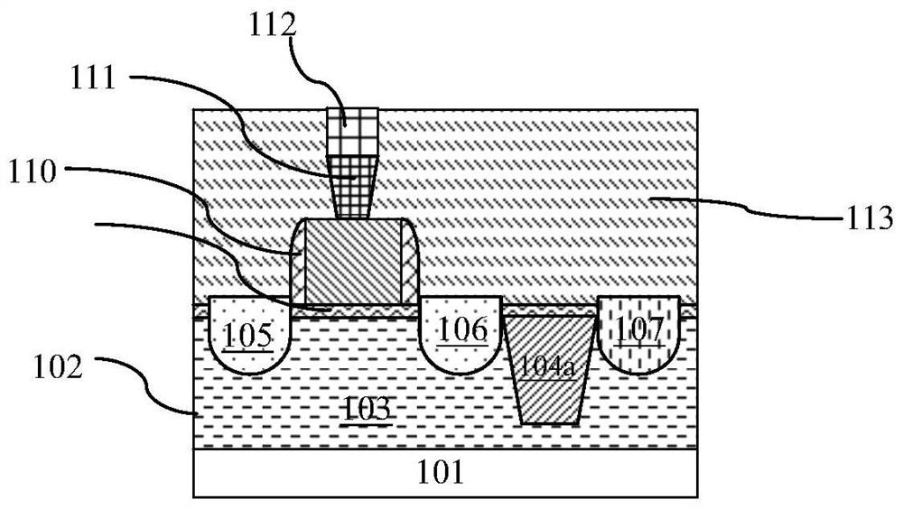
[0066] Such as image 3 As shown, it is a schematic structural diagram of the FinFET in the embodiment of the present invention; in the parasitic capacitance test structure of the FinFET in the embodiment of the present invention, the FinFET 301 includes a gate structure, a lightly doped source region composed of a lightly doped region of the first conductivity type and Shallowly doped drain region, sidewall 210, source region 205 and drain region 206 composed of heavily doped region of the first conductivity type, well region 203 of second conductivity type and body lead-out region composed of heavily doped region of the second conductivity type District 207.

[0067] The gate structure is formed by stacking a gate dielectric layer 208 and a gate conductive material layer 209 .

[0068] The second conductivity type well region 203 is formed in the fin body 202 . In the embodiment of the present invention, the fin body 202 is formed by patterning and etching a semiconductor ...


PUM


Abstract

The invention discloses a parasitic capacitance test structure of a FinFET. The FinFET comprises a gate structure, a lightly doped source region and a lightly doped drain region which are formed by a first conductive type lightly doped region, a side wall, a source region and a drain region which are formed by a first conductive type heavily doped region, a second conductive type well region and a body lead-out region which is formed by a second conductive type heavily doped region. The number of the parasitic capacitance test structures of the FinFET is multiple, and first conductive type well regions are formed in fin bodies in forming areas of the multiple parasitic capacitance testing structures. A first test structure in the parasitic capacitance test structure is formed by replacing the second conductive type well regions of the FinFET with first conductive type well regions and removing thelightly doped source region and the lightly doped drain region at the same time. The invention also discloses a parasitic capacitance test method of the FinFET. Butterfly defects can be prevented, mass production can be facilitated, and calculation of stray capacitance of the zeroth metal layer and the zeroth through hole and the electrical thickness of the gate dielectric layer can be conveniently achieved.

Description

technical field [0001] The invention relates to the field of semiconductor integrated circuit manufacturing, in particular to a FinFET parasitic capacitance testing structure. The invention also relates to a method for testing the parasitic capacitance of the FinFET. Background technique [0002] The gate structure of FinFET usually adopts a metal gate (MG), and the gate dielectric layer usually includes a high dielectric constant layer (HK). The electrical thickness of the gate dielectric layer usually needs to be tested and extracted through the capacitance of the gate. Such as figure 1 As shown, it is a schematic structural diagram of the existing FinFET; the existing FinFET includes: the FinFET includes a gate structure, a lightly doped source region and a shallowly doped drain region composed of a lightly doped region of the first conductivity type, sidewalls 110, and A source region 105 and a drain region 106 composed of a heavily doped region of the first conductivi...

Claims


Application Information

Patent Timeline
Patent Type & Authority Applications(China)
IPC IPC(8): H01L23/544H01L21/66
CPCH01L22/34H01L22/30H01L22/14
Inventor 汪雪娇石晶徐翠芹刘巍
Owner SHANGHAI HUALI INTEGRATED CIRCUTE MFG CO LTD
Learn More