Supercharge Your Innovation With Domain-Expert AI Agents!

Method for manufacturing silicon-based OLED pixel photoetching internally-tangent structure

A manufacturing method and pixel light technology, applied in microlithography exposure equipment, optics, optomechanical equipment, etc., can solve problems such as poor precision and stability

Pending Publication Date: 2022-02-11
YUNNAN NORTH OLIGHTEK OPTO ELECTRONICS TECH
View PDF0 Cites 0 Cited by
  • Summary
  • Abstract
  • Description
  • Claims
  • Application Information

AI Technical Summary

Problems solved by technology

[0005] Aiming at the problem of poor accuracy and stability of the silicon-based OLED anode pixel photolithography inscribed structure produced by the traditional process, the present invention proposes a silicon-based OLED pixel photolithography inscribed structure manufacturing method

Method used


Image

  • Method for manufacturing silicon-based OLED pixel photoetching internally-tangent structure
  • Method for manufacturing silicon-based OLED pixel photoetching internally-tangent structure
  • Method for manufacturing silicon-based OLED pixel photoetching internally-tangent structure

Examples


Embodiment 1

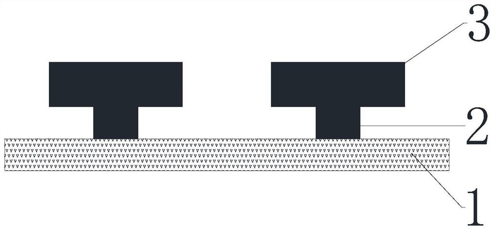
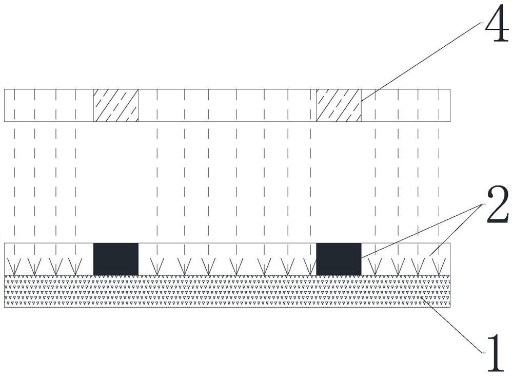
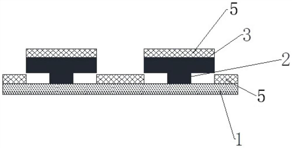
[0039] Embodiment 1: The fabrication method of silicon-based OLED pixel photolithography inscribed structure consists of the following steps:

[0040] Step 1): Coat the 8-inch silicon wafer with a layer Thick positive photoresist B-PR; use a 0.5-1.0 micron line width mask and an i-line photolithography machine with 100-200msec energy to expose the silicon wafer;

[0041] Step 2): Apply a second coating on the exposed silicon wafer; spin coat a layer on the positive photoresist B-PR Thick positive photoresist T-PR; use 0.5-1.5 micron line width mask, 100-200msec energy i-line photolithography machine to perform secondary exposure on silicon wafers;

[0042] Step 3): Take the exposed silicon wafer to a developing machine for developing, the developing temperature is 80-100°C, and the developing time is 150-200s;

[0043] Step 4): Carry out metal anode evaporation on the silicon wafer, the thickness of the anode layer

[0044] Step 5): peel off the silicon wafer that has b...


PUM


Abstract

The invention provides a method for manufacturing a silicon-based OLED pixel photoetching internally tangent structure. The method comprises the following steps: a, coating glue for the first time: coating Bottom-Photoresist at the bottom of a silicon wafer; b, performing primary exposure: performing primary exposure on the silicon wafer coated with the positive photoresist by using a photoetching machine; c, performing second time of glue coating: carrying out top positive photoresist (Top-Photoresist) coating on the silicon wafer; d, performing secondary exposure: performing secondary exposure on the silicon wafer coated with the photoresist by using the photoetching machine; e, performing developing: carrying out primary developing on the glued silicon wafer on a developing machine. The method is used for preparing an internally-tangent structure in an anode pixel photoetching process and manufacturing a high-resolution anode pixel; the manufacturing process is simple, the ideal anode pixel photoetching inscribed structure is directionally manufactured by using the photosensitive material for multiple times of gluing, exposure and development, and the problems of bottom layer morphology epitaxy, low metal anode resolution and metal anode adhesion caused by poor stability in the development process after one-time exposure in the traditional process are effectively avoided.

Description

technical field [0001] The invention relates to the field of manufacturing OLED metal anode pixels, in particular to a method for manufacturing a silicon-based OLED pixel photolithography inscribed structure. Background technique [0002] The invention relates to a silicon-based oled anode pixel photoetching inscribed structure manufacturing method, which uses the difference in solubility of positive photoresist before and after exposure in the developer to produce an ideal inscribed structure; the traditional process usually starts at the bottom of the silicon wafer. Coat the bottom stripping glue, which is non-photosensitive and soluble in the developer; then coat a top layer of photoresist; and then expose through a set of specific pattern masks. Under the action of photons, the photosensitive compound decomposes and stimulates photochemical reactions. After exposure, develop, the top photoresist: the positive photoresist on the exposed part will react with the developer ...

Claims


Application Information

Patent Timeline
IPC IPC(8): H01L51/52H01L51/56G03F7/20G03F7/095
CPCG03F7/095G03F7/2022H10K50/81H10K71/00
Inventor 杨炜平保加兵杨丽丽杜浩楠刘佰红梁翔石春明殷艳娥杨晓雪马跃霞
Owner YUNNAN NORTH OLIGHTEK OPTO ELECTRONICS TECH
Features
  • R&D
  • Intellectual Property
  • Life Sciences
  • Materials
  • Tech Scout
  • Unparalleled Data Quality
  • Higher Quality Content
  • 60% Fewer Hallucinations
Learn More