Operational amplifier and output stage circuit thereof

An output stage circuit and output voltage technology, applied in the direction of amplifier input/output impedance improvement, amplifier, differential amplifier, etc., can solve the problems of slow output response speed, large output impedance, poor stability, etc., to reduce output impedance and improve circuit The stability and the effect of improving the transient response speed

Active Publication Date: 2022-02-11
杭州深谙微电子科技有限公司
View PDF13 Cites 0 Cited by
  • Summary
  • Abstract
  • Description
  • Claims
  • Application Information

AI Technical Summary

Problems solved by technology

If you want to use medium voltage components to implement a voltage regulator, the output voltage range of the voltage regulator must be limited, otherwise the voltage across the output transistor may exceed its withstand voltage, which limits the further reduction of the supply voltage to a certain extent , which is not applicable in some low-voltage applications; on the other hand, the output impedance of the output stage itself is relatively large. When the load current jumps, not only the output response speed is slow, but also there is a large value jump, and the stability is poor

Method used


Image

  • Operational amplifier and output stage circuit thereof
  • Operational amplifier and output stage circuit thereof
  • Operational amplifier and output stage circuit thereof

Examples


Embodiment 1

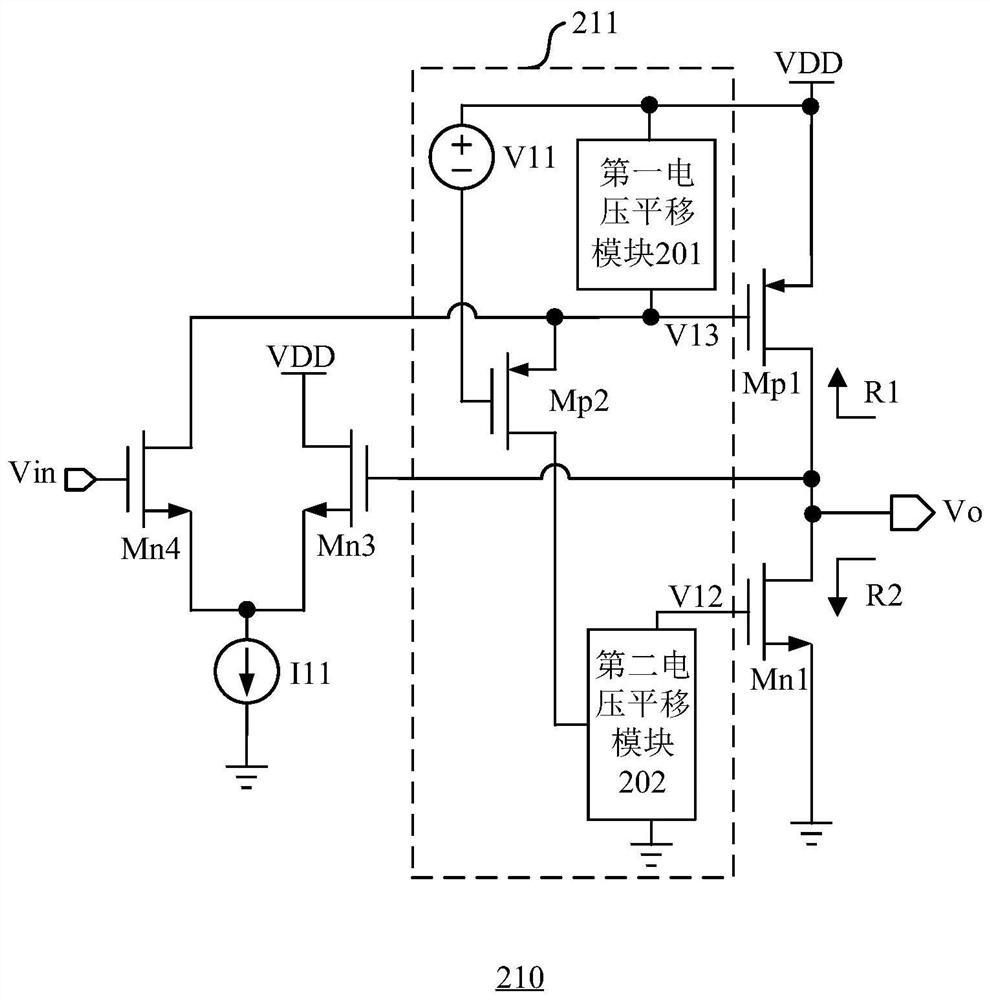
[0057] figure 2 A schematic structural diagram of the output stage circuit provided by Embodiment 1 of the present disclosure is shown, Figure 3a show figure 2 A schematic diagram of a voltage translation circuit in an embodiment of the shown output stage circuit, Figure 3b show figure 2 A schematic diagram of a voltage translation circuit in another embodiment of the shown output stage circuit.

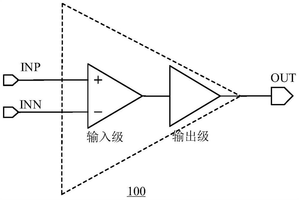
[0058] refer to figure 2 , the output stage circuit 210 provided in Embodiment 1 of the present disclosure includes:

[0059] The output transistor pair includes a first transistor Mp1 and a second transistor Mn1 connected in series between the power supply terminal and the ground, and the connection node of the first transistor Mp1 and the second transistor Mn1 is used as the output terminal of the output stage circuit 210 for Provide output voltage Vo;

[0060] The bias voltage generator 211 has a first output terminal providing the first bias voltage V13 and a second o...

Embodiment 2

[0081] Figure 3c A schematic structural diagram of the output stage circuit provided by Embodiment 2 of the present disclosure is shown.

[0082] combine Figure 2 ~ Figure 3c , the basic structure of the output stage circuit 210 provided by the second embodiment of the present disclosure is the same as that of the first embodiment, the difference is:

[0083] In the bias voltage generator 211, the first voltage translation module 201 includes a first resistor R12, and the first resistor R12 is connected between the first terminal and the control terminal of the aforementioned first transistor Mp1 for The power supply voltage VDD is divided at the control terminal of the first transistor Mp1 to form the first bias voltage V13; the second voltage translation module 202 includes a third current source I14 connected to the first bias voltage V14. Between the second end of the fifth transistor Mp2 and the ground, and the connection node between the fifth transistor Mp2 and the ...

Embodiment 3

[0085] Figure 3d A schematic structural diagram of the output stage circuit provided by Embodiment 3 of the present disclosure is shown.

[0086] combine Figure 2 ~ Figure 3d , the basic structure of the output stage circuit 210 provided by Embodiment 3 of the present disclosure is the same as that of Embodiment 2 above, except that:

[0087] In the bias voltage generator 211, the second voltage translation module 202 includes a second resistor R11, the second resistor R11 is connected between the second terminal of the aforementioned fifth transistor Mp2 and the ground, and the fifth transistor Mp2 is connected to the aforementioned The connection node of the second resistor R11 is used as the aforementioned second output terminal for forming the aforementioned second bias voltage V12 when the fifth transistor Mp2 is turned on.


PUM


Abstract

The invention provides an operational amplifier and an output stage circuit thereof, the output stage circuit can utilize an output transistor pair to provide an output voltage, respectively access an intermediate signal and the output voltage provided by a preceding stage circuit through an input transistor pair, utilize a bias voltage generator to obtain the circuit state of the input transistor pair, and generate a first bias voltage and a second bias voltage and respectively provide the first bias voltage and the second bias voltage to the control end of the output transistor pair, wherein the bias voltage generator is used for forming a feedback control loop of the output voltage by using the input transistor pair so as to realize transient response of the output voltage to load change. Therefore, the power supply voltage range of the output stage circuit can be expanded, the output impedance of the output stage circuit can be reduced, and the transient response speed to a load and the stability of the circuit can be improved.

Description

technical field [0001] The present disclosure relates to the technical field of integrated circuits, in particular to an operational amplifier and its output stage circuit. Background technique [0002] A high-performance amplifier has the characteristics of high gain and low output impedance. It can amplify tiny signals and drive small impedance loads, and has strong drive capability. In general amplifier design often such as Figure 1a As shown, it can be divided into input stage and output stage. The input stage provides a large voltage gain, and the output stage provides high current drive capability with a small output impedance. How to reduce the output impedance of the output stage and drive a smaller load has always been one of the key points and difficulties in circuit design. In addition, the output stage of the amplifier requires both the ability to output current and the ability to absorb current, so it generally consists of a pair of heteropolar transistor pai...

Claims


Application Information

Patent Timeline
Patent Type & Authority Applications(China)
IPC IPC(8): H03F1/56H03F3/45
CPCH03F1/56H03F3/45179
Inventor 陈雷铖卫梦昭孙恬静
Owner 杭州深谙微电子科技有限公司
Why Eureka
Try Eureka