Semiconductor packaging structure and manufacturing method thereof
A packaging structure and semiconductor technology, applied in the fields of semiconductor/solid-state device manufacturing, semiconductor devices, semiconductor/solid-state device components, etc., can solve the problems of limited power transmission capacity, insertion loss, limited through-silicon via process capability, etc. The effect of improving power transmission capacity and reducing insertion loss
- Summary
- Abstract
- Description
- Claims
- Application Information
AI Technical Summary
Problems solved by technology
Method used
Image

Examples
Embodiment Construction
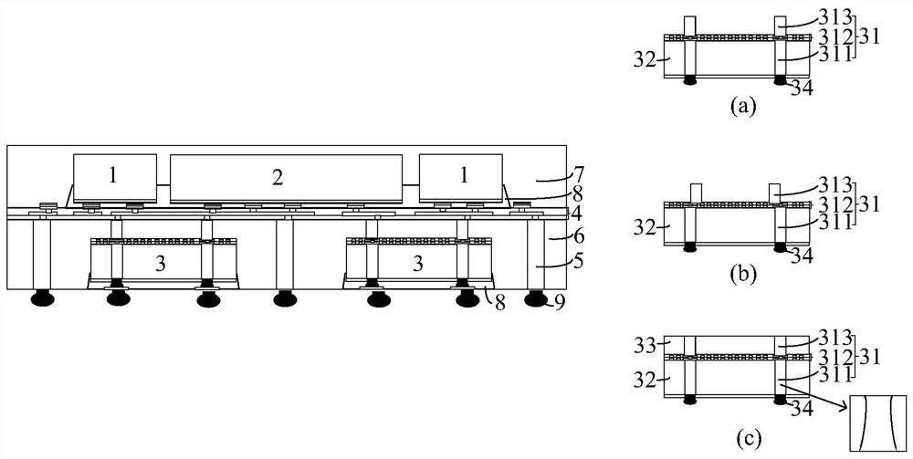
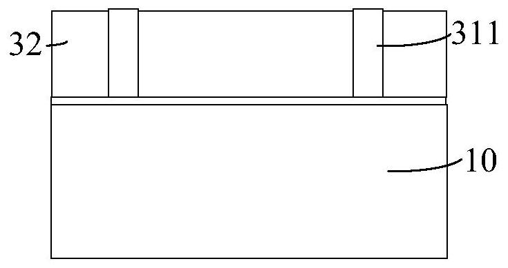
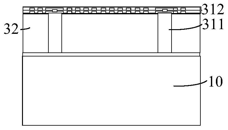
[0051] The specific implementation manners of the present disclosure will be described below in conjunction with the accompanying drawings and examples. Those skilled in the art can easily understand the technical problems solved by the present disclosure and the technical effects produced through the contents recorded in this specification. It should be understood that the specific embodiments described here are only used to explain related inventions, rather than to limit the invention. In addition, for the convenience of description, only the parts related to the related invention are shown in the drawings.
[0052] It should be noted that the structures, proportions, sizes, etc. shown in the accompanying drawings of the specification are only used to match the content recorded in the specification for the understanding and reading of those skilled in the art, and are not intended to limit the implementation of the present disclosure. There are limited conditions, so it has...
PUM
 Abstract
Description
Claims
Application Information
 - R&D
- Intellectual Property
- Life Sciences
- Materials
- Tech Scout
- Unparalleled Data Quality
- Higher Quality Content
- 60% Fewer Hallucinations
Browse by: Latest US Patents, China's latest patents, Technical Efficacy Thesaurus, Application Domain, Technology Topic, Popular Technical Reports.
© 2025 PatSnap. All rights reserved.Legal|Privacy policy|Modern Slavery Act Transparency Statement|Sitemap|About US| Contact US: help@patsnap.com