Centralized control method and system for interconnection among multiple FPGA chips
A centralized control and control system technology, applied in the field of communication, can solve problems such as low speed, difficult to meet complex system control requirements, difficult to meet control timing requirements, etc., to achieve the effect of increasing line speed
- Summary
- Abstract
- Description
- Claims
- Application Information
AI Technical Summary
Problems solved by technology
Method used
Image

Examples
specific Embodiment approach
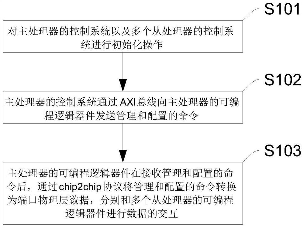
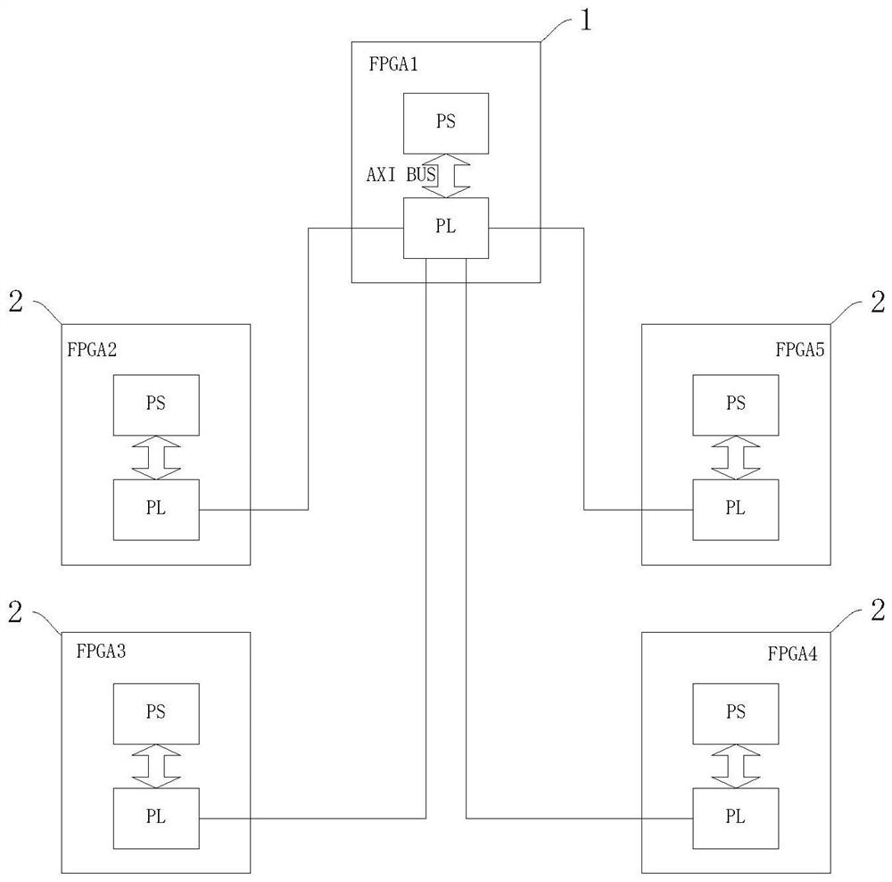
[0031] see figure 1 , figure 2 and Figure 4 , a centralized control method for the interconnection of multiple FPGA chips provided by the embodiment of the present application. The present invention proposes a high-speed centralized control method based on the interconnection of programmable logic devices in the processor. The principle is to use the main The programmable logic device of processor 1 (hereinafter referred to as PL) uniformly configures the programmable logic device of slave processor 2, and the original control system of slave processor 2 (control system hereinafter referred to as PS) is only used for system initialization Some initialization configurations, thereby increasing the line speed, and satisfying the complex control and management of the system of massive antenna technology (Massive MIMO system), the line rate can reach 4GHz. Its specific implementation is as follows:
[0032]The hardware of the present invention is all based on the Xilinx ZYNQ...
Embodiment 2
[0053] see Figure 5 , a centralized control system interconnected among multiple FPGA chips, including:
[0054] The processor module 3 is used for the main processor 1 and multiple slave processors 2 centrally controlled by the main processor 1; the initialization module 4 is used for controlling the control system of the main processor 1 and multiple slave processors 2 The system performs an initialization operation; the configuration module 5 is used for the control system of the main processor 1 to send management and configuration commands to the programmable logic device of the main processor 1 through the AXI bus; the inter-chip interaction module 6 is used for the main processor 1 After receiving the management and configuration commands, the programmable logic device converts the management and configuration commands into port physical layer data through the chip2chip protocol, and performs data interaction with multiple slave processors 2 respectively.
Embodiment 3
[0056] see Figure 4 , an electronic device comprising a main processor 1, a plurality of slave processors 2 connected to the main processor 1, at least one memory and a data bus; wherein: the main processor 1, a plurality of slave processors 2, and the memory through The data bus completes mutual communication; the memory stores program instructions that can be executed by the processor, and the master processor 1 and multiple slave processors 2 call the program instructions to execute a centralized control method for interconnecting multiple FPGA chips. Example implementation:
[0057] The main processor 1 and multiple slave processors 2 centrally controlled by the main processor 1; the control system of the main processor 1 and the control systems of multiple slave processors 2 are initialized; the control system of the main processor 1 passes The AXI bus sends management and configuration commands to the programmable logic device of the main processor 1; after receiving t...
PUM
 Abstract
Description
Claims
Application Information
 - R&D
- Intellectual Property
- Life Sciences
- Materials
- Tech Scout
- Unparalleled Data Quality
- Higher Quality Content
- 60% Fewer Hallucinations
Browse by: Latest US Patents, China's latest patents, Technical Efficacy Thesaurus, Application Domain, Technology Topic, Popular Technical Reports.
© 2025 PatSnap. All rights reserved.Legal|Privacy policy|Modern Slavery Act Transparency Statement|Sitemap|About US| Contact US: help@patsnap.com