Multi-chip fan-out type packaging method and packaging structure

A packaging method and a fan-out technology, which is applied in the manufacture of electrical components, electrical solid devices, semiconductor/solid devices, etc., can solve the problems of not being able to fully reflect the advantages of thin packaging, increase the thickness of the package, and reduce the purchase of machines , Reduce production costs and improve economic benefits

Pending Publication Date: 2022-02-18
江苏芯德半导体科技有限公司
View PDF0 Cites 0 Cited by
  • Summary
  • Abstract
  • Description
  • Claims
  • Application Information

AI Technical Summary

Problems solved by technology

[0004] However, the existing fan-out package has problems such as substrate, interposer and underfill, which increases the thickness of the package body and cannot fully reflect the advantages of thin package.

Method used


Image

  • Multi-chip fan-out type packaging method and packaging structure
  • Multi-chip fan-out type packaging method and packaging structure
  • Multi-chip fan-out type packaging method and packaging structure

Examples


Embodiment

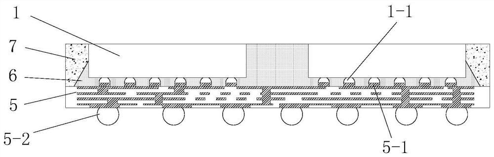
[0040] As shown in Figure 2, a multi-chip fan-out packaging method in this embodiment includes the following steps:

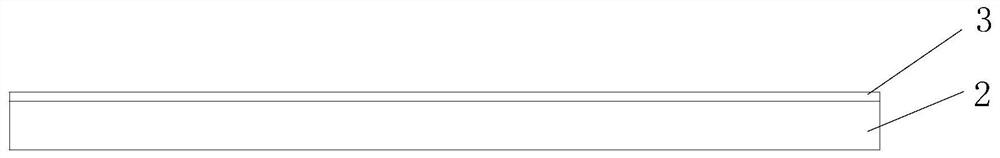
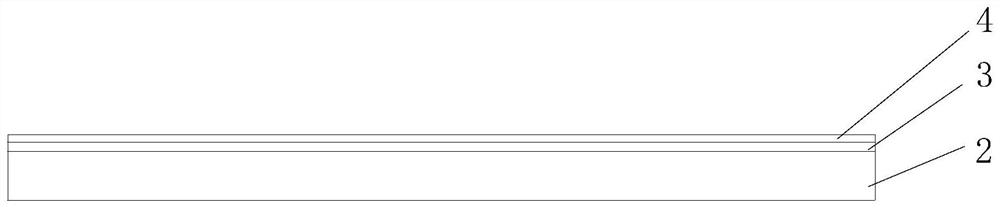
[0041] Step 1, see Figure 2a with Figure 2b As shown, a composite separation layer 3 is coated on the surface of the transparent carrier 2, and then a metal layer 4 with a certain thickness is sputtered on the composite separation layer 3;

[0042] Step two, see Figure 2c As shown, the rewiring metal circuit layer 5 and the corresponding upper layer metal pad 5-1 are formed on the metal layer 4 by multiple photolithography, sputtering and electroplating;

[0043] Step 3, after thinning the chip 1 as a whole to the target thickness, dicing is performed, and then chip pads 1-1 are made on the bottom of each independent chip 1;

[0044] Step 4, see Figure 2d with Figure 2e As shown, a plurality of chips 1 are welded to the upper metal pad 5-1 of the rewiring metal circuit layer 5 through the chip pad 1-1, and the gap between the pads is underfilled to fo...


PUM


Abstract

The invention discloses a multi-chip fan-out type packaging method and packaging structure. The method comprises steps of sequentially manufacturing a composite separation layer and a metal layer on a transparent support plate, forming a rewiring metal line layer and a corresponding metal bonding pad on the metal layer, welding chips to the rewiring metal line layer, and carrying out filling of the chips to form a filling layer; processing to obtain a plastic package wafer after a package body is formed through plastic package, removing the metal layer through corrosion and other processing, forming a bottom layer metal bump at the bottom of the rewiring metal line layer, and communicating the bottom layer metal bump with a lead at the bottom of the rewiring metal line layer; and finally, integrally thinning the processed plastic package wafer, pasting a film, and cutting into a plurality of single independent package bodies.

Description

technical field [0001] The invention belongs to semiconductor packaging technology, in particular to a multi-chip fan-out packaging method and packaging structure. Background technique [0002] With the development of integrated circuits, the degree of integration continues to increase, and the number of transistors contained in each chip also increases continuously. In order to ensure a small chip area, the number of pins cannot be accommodated in the chip, so a fan-out packaging method is derived. [0003] The fan-out package leads the I / O from the inside of the chip to the outside of the chip through rewiring technology, which solves the problem of interconnection between the packaged chip and the printed circuit board. This method reduces power consumption, weight ratio and product cost while ensuring function, interconnection and reliability, and continuously expands its application field. It is currently a highly competitive technical solution. [0004] However, exis...

Claims


Application Information

Patent Timeline
Patent Type & Authority Applications(China)
IPC IPC(8): H01L21/50H01L21/56H01L21/60H01L23/31
CPCH01L21/50H01L21/561H01L21/568H01L24/97H01L23/3107H01L2224/97
Inventor 潘明东许连军陈益新徐海
Owner 江苏芯德半导体科技有限公司
Why Eureka
Try Eureka