Chip embedded-type encapsulation structure with reinforcing structure and encapsulation method of same

A technology to strengthen the structure and packaging structure, which is applied in the direction of electrical components, electrical solid devices, circuits, etc., can solve the problem of increasing the mismatch probability of interconnection spacing and heat dissipation difficulties, which is not conducive to the integrated development of portable electronic equipment, and the thickness of the packaging structure cannot be reduced, etc. Problems, achieve the effect of strengthening strength, realizing miniaturization, and reducing equipment requirements

Inactive Publication Date: 2016-02-03
JIANGYIN CHANGDIAN ADVANCED PACKAGING CO LTD
View PDF13 Cites 9 Cited by
  • Summary
  • Abstract
  • Description
  • Claims
  • Application Information

AI Technical Summary

Problems solved by technology

[0003] 1. The existing wafer-level chip fan-out packaging structure requires substrates (1-6) to achieve fan-out, and for small chips with high pin counts, multi-layer substrates (1-6) are required to be fan-out multiple times to be compatible with printing The completion of the interconnection on the circuit board not only increases the mismatch probability of the ever-increasing interconnection pitch and heat dissipation difficulties, but also reduces the reliability of the product, and the existence of the substrate (1-6) makes the thickness of the entire package structure unable to be reduced. The body thickness of the existing wafer-level chip fan-out packaging structure is 700-1500 microns;
[0004] 2. The existing wafer-level chip fan-out packaging structure requires the substrate (1-6) to realize fan-out, which often limits the addition of various chips with different functions, which is not conducive to the integrated development of portable electronic devices

Method used


Image

  • Chip embedded-type encapsulation structure with reinforcing structure and encapsulation method of same
  • Chip embedded-type encapsulation structure with reinforcing structure and encapsulation method of same
  • Chip embedded-type encapsulation structure with reinforcing structure and encapsulation method of same

Examples


Embodiment 1

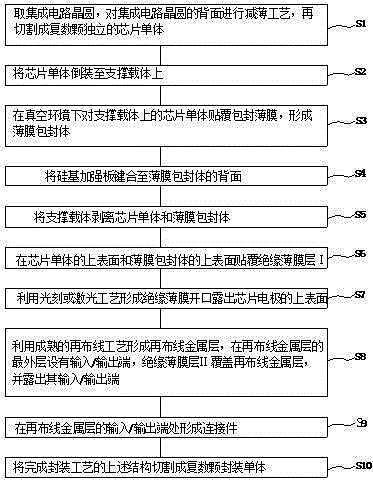
[0075] Embodiment one, see Figure 3A and Figure 3B

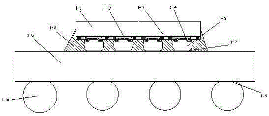
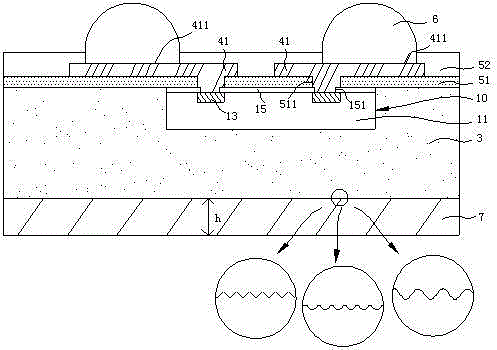
[0076] Figure 3A It is a schematic cross-sectional view of Embodiment 1 of a chip-embedded packaging structure with a reinforced structure in the present invention. The chip-embedded packaging structure of the present invention includes a chip unit 10 with a film encapsulation body 3 embedded in the back, and the chip unit 10 The upper surface of the chip body 11 is provided with a chip electrode 13 and its corresponding circuit layout, the chip surface passivation layer 15 covers the upper surface of the chip body 11 and has a chip surface passivation layer opening 151, and the upper surface of the chip electrode 13 exposes the chip The surface passivation layer opens 151 . The material of the film envelope 3 includes but is not limited to epoxy molding compound, which is generally made of high-performance phenolic resin as a curing agent, silicon micropowder as a filler, and various additives. It is in a molten stat...

Embodiment 2

[0095] Embodiment two, see Figure 5A and Figure 5B

[0096] The number of chip monomers can be more than one, and more chip packages with different functions can be realized by adopting chip packaging system collaborative design.

[0097] Figure 5AIt is a schematic cross-sectional view of Embodiment 2 of a chip-embedded packaging structure with a reinforced structure of the present invention. The chip-embedded packaging structure of the present invention includes two chip units 10 and a chip unit whose backs are embedded in a film encapsulation body 3 20, its upper surface is generally arranged flush. The material of the film envelope 3 includes but is not limited to epoxy molding compound, which is generally made of high-performance phenolic resin as a curing agent, silicon micropowder as a filler, and various additives. It is in a molten state at 185°C, and tightly wraps the front, rear, left, and right sides and the back of the chip unit 10. After cooling, it will gr...

Embodiment 3

[0101] Embodiment three, see Figure 6

[0102] The packaging structure of Embodiment 3 is similar to that of Embodiment 1 and Embodiment 2, the difference is that the rewiring metal layer 41 can also be two or more layers to form a plurality of rewiring process layers, so as to realize a multi-layer fan-out packaging structure ,Such as Figure 6 shown. The multi-layer rewiring process layer is an example of three layers, including a rewiring metal layer 41, a rewiring metal layer 43, and a rewiring metal layer 45 to meet the multi-information communication. The wiring process layers are matched, and they are respectively arranged in it to play the roles of insulation, protection, reinforcement, etc. The insulating film layer II 52 is generally made of polymeric organic insulating materials such as epoxy resin and polyimide. The outermost layer of the multi-layer redistribution process layer is provided with input / output terminals, and the number of input / output terminals ...


PUM


Abstract

The invention discloses a chip embedded-type encapsulation structure with a reinforcing structure and an encapsulation method of the same, which belong to the technical field of semiconductor encapsulation. The chip embedded-type encapsulation structure with the reinforcing structure comprises chip single bodies and a thin film encapsulating body, wherein one or more than one chip single bodies are embedded from the back face into the thin film encapsulating body, the upper surfaces of the chip single bodies and the upper surface of the thin film encapsulating body are covered by an insulated thin film layer I, an opening of the insulated thin film layer I is disposed in the upper surface of a chip electrode, a re-wiring metal layer is formed on the upper surface of the insulated thin film layer, the re-wiring metal layer is respectively electrically connected to the chip electrodes, an input end/output end is disposed on the outmost layer of the re-wiring metal layer, a connecting part is formed at the input end/output end, and the back face of the thin film encapsulating body is equipped with a silicon substrate reinforcing plate. The encapsulation method disclosed by the invention reduces thicknesses of products, increases product reliability and realizes the multi-chip encapsulation structure through wafer-level technological forming.

Description

technical field [0001] The invention relates to a chip embedded packaging structure with a strengthening structure and a packaging method thereof, belonging to the technical field of semiconductor packaging. Background technique [0002] With the development of semiconductor silicon technology, the critical size of the chip is getting smaller and smaller. In order to reduce the cost, the more advanced chip manufacturing process with higher integration level tends to be selected when making the chip, which makes the size of the chip more and more Smaller, the I / O density on the chip surface is getting higher and higher. However, at the same time, the manufacturing process and surface mount technology of printed circuit boards have not been greatly improved. For such a chip with relatively high I / O density, if wafer-level packaging is performed, in order to ensure that the chip to be packaged and the printed circuit board can form an interconnection, the high-density I / O must...

Claims


Application Information

Patent Timeline
Patent Type & Authority Applications(China)
IPC IPC(8): H01L23/31H01L23/535H01L23/12H01L21/56H01L21/60
CPCH01L21/568H01L24/96H01L24/97H01L2224/04105H01L2224/12105H01L2224/16225H01L2224/19H01L2224/32225H01L2224/73204H01L2924/15311H01L2924/3511H01L2924/00H01L2924/00012
Inventor 张黎龙欣江赖志明陈栋陈锦辉
Owner JIANGYIN CHANGDIAN ADVANCED PACKAGING CO LTD
Why Eureka
Try Eureka