Check patentability & draft patents in minutes with Patsnap Eureka AI!

Integrated circuit mask layout, pattern correction method and mask thereof

An integrated circuit and mask technology, applied in the field of integrated circuit mask layout, can solve the problem of inability to obtain a process window, and achieve the effect of a good process window

Pending Publication Date: 2022-02-22
SHANGHAI HUALI INTEGRATED CIRCUTE MFG CO LTD
View PDF0 Cites 0 Cited by
  • Summary
  • Abstract
  • Description
  • Claims
  • Application Information

AI Technical Summary

Problems solved by technology

[0003] In the manufacturing process of Fin Field Effect Transistor (FinFet), there is a layout of a mask, such as figure 1 As shown, the active area (CAA) of the mandrel structure and the 45-degree sealing ring (seal ring) keep a fixed distance, so that the active area (CAA) and the overhang of the alignment mark AA are not same, resulting in the inability to obtain the ideal process window

Method used


Image

  • Integrated circuit mask layout, pattern correction method and mask thereof
  • Integrated circuit mask layout, pattern correction method and mask thereof

Examples


Embodiment 1

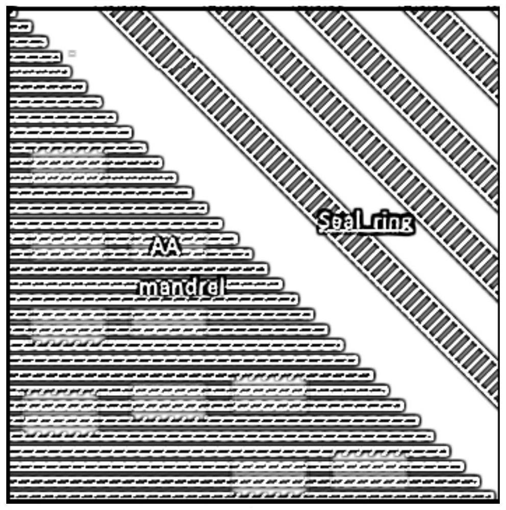
[0025] This embodiment provides a layout of an integrated circuit mask. The layout includes the graphics required in various photolithography processes. The improvement of the present invention lies in the relationship between the active area graphics, the sealing ring graphics and the two graphics, and other graphics. It is a prior art, so it will not be repeated in the embodiment.

[0026] Such as figure 2 As shown, the integrated circuit mask layout of this embodiment includes a plurality of active region patterns 1 and a plurality of sealing ring patterns 2;

[0027] The active region pattern 1 is parallel to the horizontal direction of the mask layout;

[0028] The sealing ring pattern 2 forms an included angle with the horizontal direction of the mask layout.

[0029] A plurality of active area patterns 1 form a group to form multiple groups of active area patterns;

[0030] Each group of active region patterns corresponds to adjacent alignment marks 3, and the edge ...

Embodiment 2

[0036] This embodiment provides a pattern correction method for an integrated circuit mask layout, and the integrated circuit mask layout is the layout in Embodiment 1.

[0037] Such as figure 2 shown. In this embodiment, the optical proximity effect correction method OPC is used to correct the original pattern of the integrated circuit mask layout, and the edge of each active region pattern 1 in the same group of active region patterns near the seal ring pattern 2 is The vertical direction of the mask layout is flush. Make the floating distance corresponding to each active area pattern 1 and the adjacent alignment mark 3 in the same group of active area patterns the same

Embodiment 3

[0039] This embodiment provides an integrated circuit mask, including the layout of the integrated circuit mask described in Implementation 1.


PUM


Abstract

The invention discloses a mask layout of an integrated circuit. The mask layout comprises a plurality of active region patterns and a plurality of sealing ring patterns; the active region pattern is parallel to the horizontal direction of the mask layout; an included angle is formed between the sealing ring pattern and the horizontal direction of the mask layout; a plurality of active region patterns form a group, and a plurality of groups of active region patterns are formed in total; each group of active region patterns corresponds to the adjacent alignment mark, and the edge of one side, close to the sealing ring pattern, of each active region pattern in the same group of active region patterns is flush in the vertical direction of the mask layout. Compared with the prior art, the mask layout and the mask manufactured by adopting the layout provided by the invention have the advantage that a better process window can be obtained in the manufacturing process of an integrated circuit.

Description

technical field [0001] The invention relates to the technical field of semiconductor integrated circuit manufacturing, in particular to an integrated circuit mask layout, a pattern correction method and a mask. Background technique [0002] In the manufacturing process of semiconductor integrated circuits, optical proximity correction (Optical Proximity Correct, OPC for short) needs to be performed on the design layout, so as to improve the manufacturability of graphics. OPC is to improve the impact of optical proximity effect on exposure, so the basic work is to cut and move the layout segment by line, and then iterate continuously, and finally verify with the actual results. [0003] In the manufacturing process of Fin Field Effect Transistor (FinFet), there is a layout of a mask, such as figure 1 As shown, the active area (CAA) of the mandrel structure and the 45-degree sealing ring (seal ring) keep a fixed distance, so that the active area (CAA) and the overhang of the ...

Claims


Application Information

Patent Timeline
IPC IPC(8): G03F1/36G03F1/42
CPCG03F1/36G03F1/42
Inventor 陈柏翰曾鼎程胡展源
Owner SHANGHAI HUALI INTEGRATED CIRCUTE MFG CO LTD
Features
  • R&D
  • Intellectual Property
  • Life Sciences
  • Materials
  • Tech Scout
  • Unparalleled Data Quality
  • Higher Quality Content
  • 60% Fewer Hallucinations
Learn More