Three-dimensional memory and forming method thereof

A memory and three-dimensional technology, which is applied in the direction of electric solid-state devices, semiconductor devices, electrical components, etc., can solve problems such as the inability to form complex patterns, and achieve the effects of ensuring shape consistency, reducing the difficulty of forming, and improving the shape

Pending Publication Date: 2022-03-01
YANGTZE MEMORY TECH CO LTD
View PDF0 Cites 0 Cited by
  • Summary
  • Abstract
  • Description
  • Claims
  • Application Information

AI Technical Summary

Problems solved by technology

[0005] The invention provides a three-dimensional memory and its forming method, which are used to solve the problem that complex patterns cannot be formed in the prior art, so as to improve the performance of the three-dimensional memory

Method used


Image

  • Three-dimensional memory and forming method thereof
  • Three-dimensional memory and forming method thereof
  • Three-dimensional memory and forming method thereof

Examples


Embodiment Construction

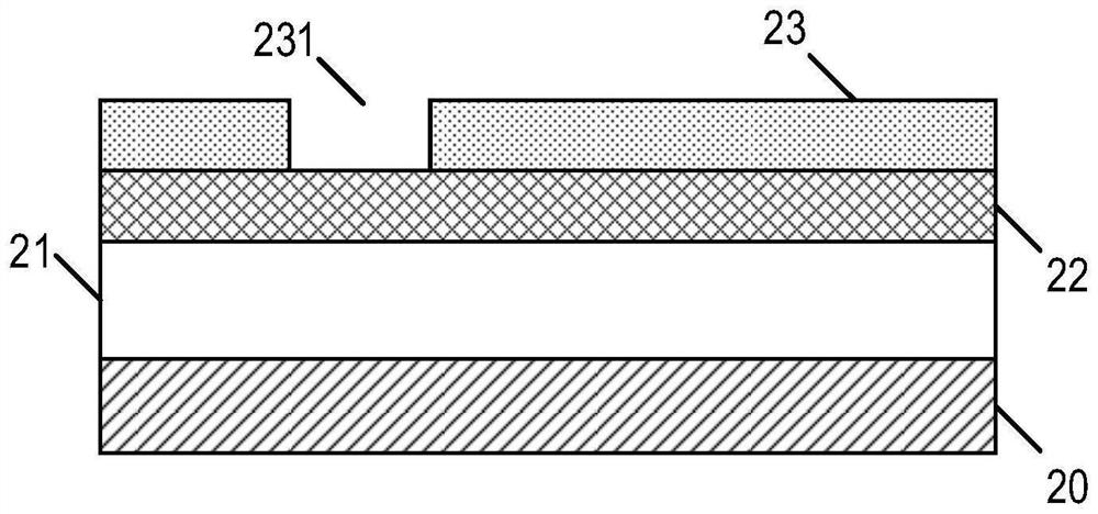
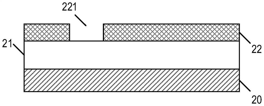
[0047] The specific implementation of the three-dimensional memory provided by the present invention and its forming method will be described in detail below in conjunction with the accompanying drawings.

[0048] Due to the limitation of the optical limit resolution and the pattern size, when forming a complex pattern including multiple sub-patterns on the photoresist layer, the boundaries between two adjacent sub-patterns are easy to connect together, for example, when forming a petal-shaped pattern, adjacent The edges of the two petals are connected together, causing the angle between two adjacent petals to be greater than 90 degrees (that is, an obtuse angle). When the complex pattern in the photoresist layer is transferred downward to the When on the wafer, the pattern formed on the wafer is basically an approximate rectangular pattern with fuzzy boundaries, and there is a large deviation from the preset shape of the complex pattern, resulting in the inability of the compl...


PUM


Abstract

The invention relates to a three-dimensional memory and a forming method thereof. The forming method of the three-dimensional memory comprises the following steps: providing a substrate; forming a first sacrificial layer including a first etching pattern on the substrate; the first etching pattern is backfilled, a second sacrificial layer comprising a second etching pattern is formed on the first sacrificial layer, and the projection of the first etching pattern intersects with the projection of the second etching pattern in the direction perpendicular to the substrate; etching the first sacrificial layer along the second etching pattern to form a third etching pattern communicated with the first etching pattern; and etching the substrate along the first etching pattern and the third etching pattern, and forming a combined pattern in the substrate. According to the invention, the morphology of the finally formed combined pattern is improved.

Description

technical field [0001] The invention relates to the technical field of semiconductor manufacturing, in particular to a three-dimensional memory and a forming method thereof. Background technique [0002] With the development of planar flash memory, the production process of semiconductors has made great progress. However, in recent years, the development of planar flash memory has encountered various challenges: physical limits, existing development technology limits, and storage electron density limits. In this context, in order to solve the difficulties encountered in planar flash memory and pursue lower production costs per unit storage unit, various three-dimensional (3D) flash memory structures have emerged, such as 3D NOR (3D or not) flash memory and 3D NAND (3D NAND) flash memory. [0003] Among them, 3D NAND memory takes its small size and large capacity as the starting point, and the design concept of highly integrated storage units stacked in three-dimensional mo...

Claims


Application Information

Patent Timeline
Patent Type & Authority Applications(China)
IPC IPC(8): H01L27/11524H01L27/11551H01L27/11519H01L27/11565H01L27/1157H01L27/11578
CPCH10B41/10H10B41/35H10B41/20H10B43/10H10B43/35H10B43/20
Inventor 张昆张雷孙昌志高庭庭
Owner YANGTZE MEMORY TECH CO LTD
Why Eureka
Try Eureka