Thin film transistor memory and preparation method thereof

A thin film transistor and memory technology, applied in the field of thin film transistor memory and its preparation, can solve the problems affecting the stability and reliability of charge storage, and achieve the effects of accelerating electronic erasing speed, not easy to leak, and strong reliability.

Inactive Publication Date: 2022-03-01
SHANGHAI INTEGRATED CIRCUIT MFG INNOVATION CENT CO LTD
View PDF7 Cites 1 Cited by
  • Summary
  • Abstract
  • Description
  • Claims
  • Application Information

AI Technical Summary

Problems solved by technology

However, this invention is a semi-floating gate memory, and part of the floating gate is directly in contact with the channel, so that the electrons trapped in the floating gate can easily flow back into the channel, thereby affecting the stability and reliability of charge storage.

Method used


Image

  • Thin film transistor memory and preparation method thereof
  • Thin film transistor memory and preparation method thereof
  • Thin film transistor memory and preparation method thereof

Examples


Embodiment Construction

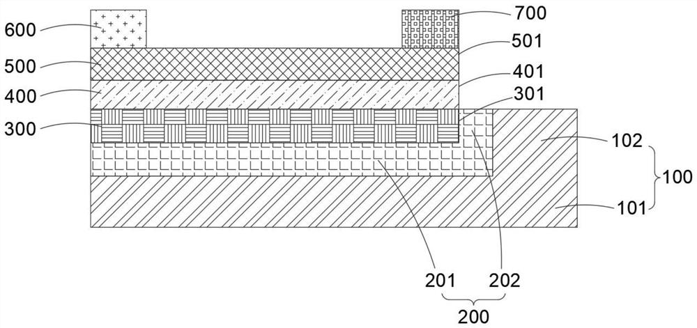
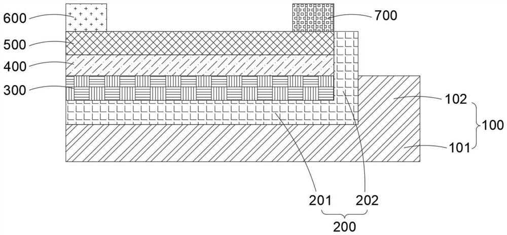
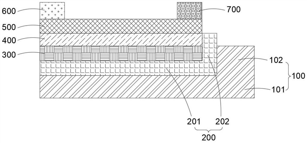
[0052] In order to make the purpose, technical solutions and advantages of the present invention clearer, the technical solutions in the embodiments of the present invention will be clearly and completely described below in conjunction with the accompanying drawings of the present invention. Obviously, the described embodiments are part of the present invention Examples, not all examples. Based on the embodiments of the present invention, all other embodiments obtained by persons of ordinary skill in the art without creative efforts fall within the protection scope of the present invention. Unless otherwise defined, the technical terms or scientific terms used herein shall have the usual meanings understood by those skilled in the art to which the present invention belongs. As used herein, "comprising" and similar words mean that the elements or items appearing before the word include the elements or items listed after the word and their equivalents, without excluding other el...


PUM


Abstract

A thin film transistor memory provided by the present invention comprises a back gate, a barrier layer, a floating gate, a tunneling layer, a channel, a source electrode and a drain electrode, the back gate comprises a bottom gate structure and a side gate structure, the side gate structure is arranged on a part of the upper surface of the bottom gate structure to form an L-shaped structure, the barrier layer is arranged on the upper surface of the bottom gate structure, and the floating gate is arranged on the upper surface of the bottom gate structure. The floating gate is arranged on the upper surface of the barrier layer, the upper surface of the floating gate is flush with the upper surface of the side gate structure, the tunneling layer is arranged on the upper surface of the floating gate, the channel is arranged on the upper surface of the tunneling layer, the source electrode and the drain electrode are arranged on the upper surface of the channel, and the side gate structure is arranged on the upper surface of the channel. According to the technical scheme, energy band regulation and control can be carried out on the floating gate through the side gate structure, so that the electronic erasing speed is increased, the electronic erasing voltage is reduced, the power consumption can be reduced, and as the channel is not in contact with the floating gate, the memory is not easy to leak and higher in reliability. The invention also provides a preparation method of the thin film transistor memory.

Description

technical field [0001] The invention relates to the technical field of semiconductor storage, in particular to a thin film transistor storage and a preparation method thereof. Background technique [0002] Non-volatile memory is an indispensable component in modern electronic devices. At present, non-volatile memory on the market is still dominated by silicon-based devices. However, due to the complex manufacturing process of traditional floating gate non-volatile memories based on single-crystal silicon substrates, usually involving high-temperature processes, it is difficult to manufacture embedded non-volatile memories on glass substrates, resulting in their Restricted when integrated into display panels. [0003] At present, a non-volatile memory based on a thin-film transistor (TFT) structure has attracted widespread attention. This memory can not only be fabricated on glass or a flexible substrate, but its manufacturing process can be well compared with the traditiona...

Claims


Application Information

Patent Timeline
Patent Type & Authority Applications(China)
IPC IPC(8): H01L29/78H01L29/423H01L21/336
CPCH01L29/66825H01L29/7841H01L29/42324
Inventor 朱宝尹睿张卫
Owner SHANGHAI INTEGRATED CIRCUIT MFG INNOVATION CENT CO LTD
Why Eureka
Try Eureka