Graphite substrate for improving wavelength uniformity of epitaxial wafer

A graphite substrate, uniformity technology, applied in the direction of single crystal growth, crystal growth, from chemically reactive gases, etc., can solve the problems of aggravated difference, uneven distribution of Mo sources, consumption, etc., to achieve volume reduction, uniform distribution, The effect of improving wavelength uniformity

Pending Publication Date: 2022-03-04
HC SEMITEK ZHEJIANG CO LTD
View PDF7 Cites 1 Cited by
  • Summary
  • Abstract
  • Description
  • Claims
  • Application Information

AI Technical Summary

Problems solved by technology

However, during the radial flow of the Mo source gas flow along the graphite substrate, the Mo source gas flow will be consumed, resulting in uneven distribution of the Mo source at different positions on the graphite substrate, so that the epitaxial wafers grown in different grooves of the graphite substrate The wavelength consistency is poor
This discrepancy is further exacerbated by the high-speed rotation of the graphite substrate

Method used


Image

  • Graphite substrate for improving wavelength uniformity of epitaxial wafer
  • Graphite substrate for improving wavelength uniformity of epitaxial wafer
  • Graphite substrate for improving wavelength uniformity of epitaxial wafer

Examples


Embodiment Construction

[0031] In order to make the purpose, technical solution and advantages of the present disclosure clearer, the implementation manners of the present disclosure will be further described in detail below in conjunction with the accompanying drawings.

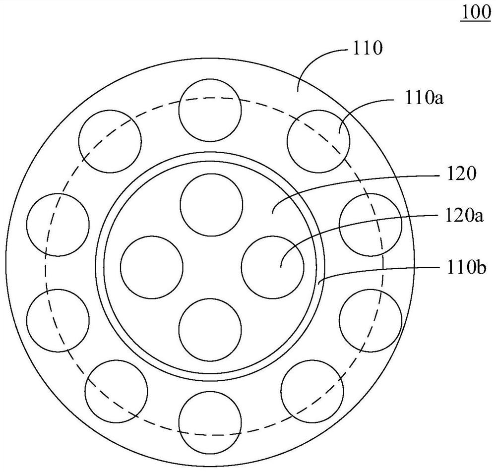
[0032] figure 1 It is a top view of a graphite substrate used to improve the wavelength consistency of an epitaxial wafer provided by an embodiment of the present disclosure, as shown in figure 1 As shown, the graphite substrate 100 includes a first substrate 110, a second substrate 120 and an exhaust device 130, and both the first substrate 110 and the second substrate 120 are discs.

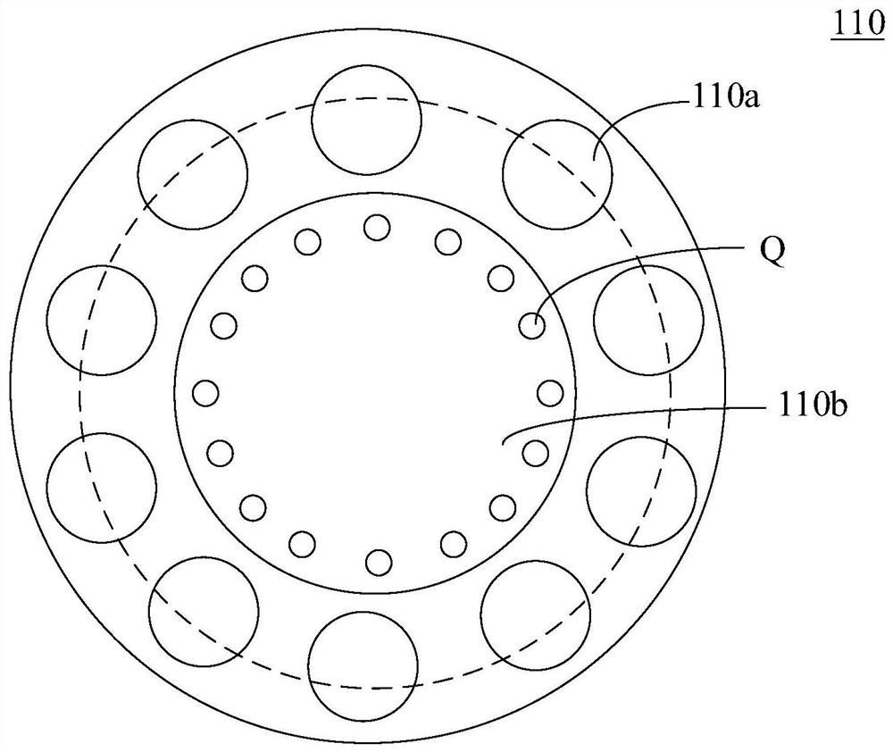
[0033] figure 2 is a top view of a first substrate provided by an embodiment of the present disclosure, such as figure 2 shown, combined with figure 1 , the upper surface of the first substrate 110 has multiple turns of first grooves 110a for accommodating the substrate, and the multiple turns of first grooves 110a are arranged on the first sub...


PUM

PropertyMeasurementUnit
thicknessaaaaaaaaaa
diameteraaaaaaaaaa
thicknessaaaaaaaaaa

Abstract

The invention provides a graphite substrate for improving the wavelength uniformity of an epitaxial wafer, and belongs to the technical field of semiconductors. The graphite base plate comprises a first base plate, a second base plate and an exhaust device, and the first base plate and the second base plate are both discs; the upper surface of the first substrate is provided with a plurality of circles of first grooves for accommodating substrates, the middle part of the first substrate is provided with a circular pit, and the bottom of the circular pit is provided with a plurality of air holes; the second substrate is coaxially arranged in the circular pit, and the upper surface of the second substrate is provided with a plurality of circles of second grooves for accommodating the substrate; and the exhaust device is configured to provide gas with set flow for the plurality of gas holes in different working states, so that the second substrate is suspended in the circular pit and is separated from the first substrate, and the second substrate and the first substrate rotate in the same direction or in the opposite direction at a set rotating speed. The epitaxial wafer grows on the graphite substrate provided by the invention, so that the wavelength uniformity of the epitaxial wafer growing in each groove of the graphite substrate can be improved.

Description

technical field [0001] The disclosure relates to the technical field of semiconductors, in particular to a graphite substrate for improving the wavelength uniformity of an epitaxial wafer. Background technique [0002] A semiconductor light-emitting diode (English: Light Emitting Diode, referred to as: LED) is a semiconductor diode that can convert electrical energy into light energy. LED has the advantages of high efficiency, energy saving, and environmental protection, and is widely used in traffic indication, outdoor full-color display and other fields. In particular, the use of high-power LEDs to realize semiconductor solid-state lighting is expected to become a new generation of light sources and enter thousands of households, causing a revolution in the history of human lighting. [0003] The epitaxial wafer is the primary product in the LED manufacturing process. When forming an epitaxial wafer, the substrate is placed on a tray in the reaction chamber of a metal or...

Claims


Application Information

Patent Timeline
Patent Type & Authority Applications(China)
IPC IPC(8): C30B25/12C30B25/14C30B25/16
CPCC30B25/12C30B25/14C30B25/165
Inventor 葛永晖陈张笑雄郭炳磊肖云飞陆香花李鹏
Owner HC SEMITEK ZHEJIANG CO LTD
Why Eureka
Try Eureka