
Delay estimation method and device of programmable logic device, equipment and storage medium

A technology for programming logic and devices, applied in computer-aided design, instrumentation, computing, etc., can solve the problems of high memory overhead of programmable logic devices, impact on performance and efficiency of routing algorithms, and large gap between delay and estimated delay, etc. Achieve the effect of improving the efficiency of routing algorithms, improving the orientation of routing expansion, and improving performance

Pending Publication Date: 2022-03-11
SHENZHEN PANGO MICROSYST CO LTD
View PDF0 Cites 0 Cited by
  • Summary
  • Abstract
  • Description
  • Claims
  • Application Information

AI Technical Summary

Problems solved by technology

[0004] The prior art usually adopts the distance estimation method or pre-traversing the netlist to calculate the delay to obtain the estimated delay value. The inventors found that the above method of obtaining the estimated delay value not only takes up more memory, but also makes the memory of the programmable logic device Expenditure is relatively large, and above-mentioned prior art scheme is when carrying out delay estimation to two internal ports (pin) that are far away in the ultra-large-scale programmable device, and the estimation accuracy of above-mentioned h value is relatively low, thereby makes distance There is a large gap between the actual delay and the estimated delay of the two distant internal ports (pins), which will have a greater impact on the performance and efficiency of the routing algorithm. Therefore, it is necessary to improve

Method used


Image

  • Delay estimation method and device of programmable logic device, equipment and storage medium
  • Delay estimation method and device of programmable logic device, equipment and storage medium
  • Delay estimation method and device of programmable logic device, equipment and storage medium

Examples


Embodiment Construction

[0040] The following will clearly and completely describe the technical solutions in the embodiments of the present invention with reference to the accompanying drawings in the embodiments of the present invention. Obviously, the described embodiments are only some, not all, embodiments of the present invention. Based on the embodiments of the present invention, all other embodiments obtained by persons of ordinary skill in the art without making creative efforts belong to the protection scope of the present invention.

[0041] The terms "first", "second", and "third" in the present invention are only used for descriptive purposes, and cannot be understood as indicating or implying relative importance or implicitly specifying the quantity of indicated technical features. Thus, features defined as "first", "second", and "third" may explicitly or implicitly include at least one of these features. In the description of the present invention, "plurality" means at least two, such a...


PUM


Abstract

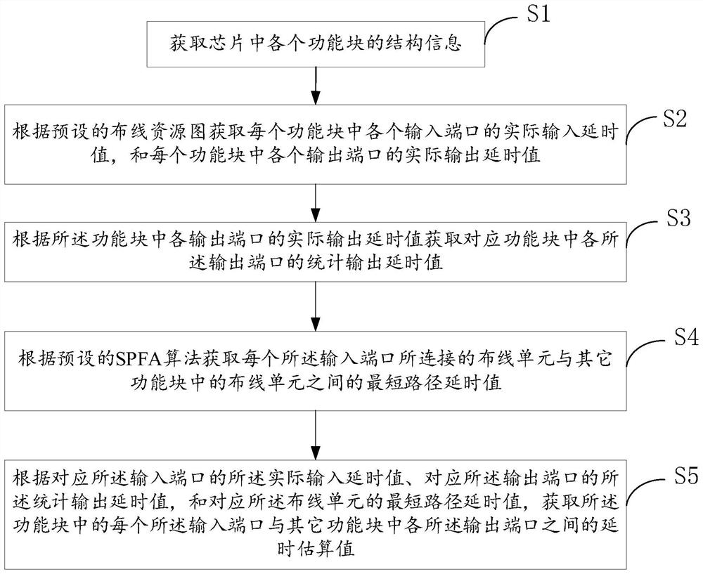
The invention discloses a delay estimation method and device of a programmable logic device, equipment and a storage medium, and belongs to the field of integrated circuit design. The method comprises the following steps: obtaining structure information of each functional block in a chip; obtaining an actual input delay value of each input port in each function block and an actual output delay value of each output port in each function block; obtaining a statistical output delay value of each output port in the corresponding function block according to the actual output delay value of each output port in the function block; obtaining a shortest path delay value between the wiring unit connected with each input port and the wiring units in other functional blocks; and obtaining a delay estimation value between each input port in the function block and each output port in other function blocks. According to the method, the memory overhead of the programmable logic device can be considered, and the method is suitable for delay estimation of a super-large-scale programmable logic device.

Description

technical field [0001] The invention belongs to the field of integrated circuit design, relates to field programmable logic device (such as FPGA chip) integrated circuit software tool design technology, in particular to a delay estimation method, device, equipment and storage medium of a programmable logic device. Background technique [0002] Such as figure 2 As shown in the schematic diagram of the delay cost model of the programmable device wiring algorithm based on the A* algorithm, in the existing routing expansion algorithm flow of the programmable device based on the A* algorithm, the delay cost model of f=g+h is often used to estimate The cost value from the current expansion node to the target node, g represents the value of the delay time that has passed from the source node to the current expansion node, plus the value of the congestion factor; h represents the estimated cost value of the delay from the current expansion node to the target node. [0003] In the a...

Claims


Application Information

Patent Timeline
Patent Type & Authority Applications(China)
IPC IPC(8): G06F30/394
CPCG06F30/394
Inventor 冯展鹏张鑫夏炜
Owner SHENZHEN PANGO MICROSYST CO LTD
Learn More