Dielectric layer for realizing multi-valued storage, resistive random access memory and preparation method and application of resistive random access memory

A technology of resistive variable memory and multi-value storage, which is applied in the direction of coating, metal material coating process, ion implantation plating, etc., can solve the problems that limit the commercial application of RRAM, and achieve low switching voltage and high resistive variable switching ratio , the effect of high abundance

Pending Publication Date: 2022-03-11
WUHAN UNIV OF TECH
View PDF0 Cites 0 Cited by
  • Summary
  • Abstract
  • Description
  • Claims
  • Application Information

AI Technical Summary

Problems solved by technology

[0006] Although the above two methods can be used to realize multi-value storage of data in RRAM, as the device size is further reduced to a few nanometers, the inevitable limitations of the above two methods limit the further commercial application of RRAM.

Method used


Image

  • Dielectric layer for realizing multi-valued storage, resistive random access memory and preparation method and application of resistive random access memory
  • Dielectric layer for realizing multi-valued storage, resistive random access memory and preparation method and application of resistive random access memory
  • Dielectric layer for realizing multi-valued storage, resistive random access memory and preparation method and application of resistive random access memory

Examples


Embodiment Construction

[0030] Specific embodiments of the present invention will be described in detail below in conjunction with the accompanying drawings. Unless otherwise stated, the raw materials and reagents used in the following examples are commercially available or can be prepared by known methods.

[0031]

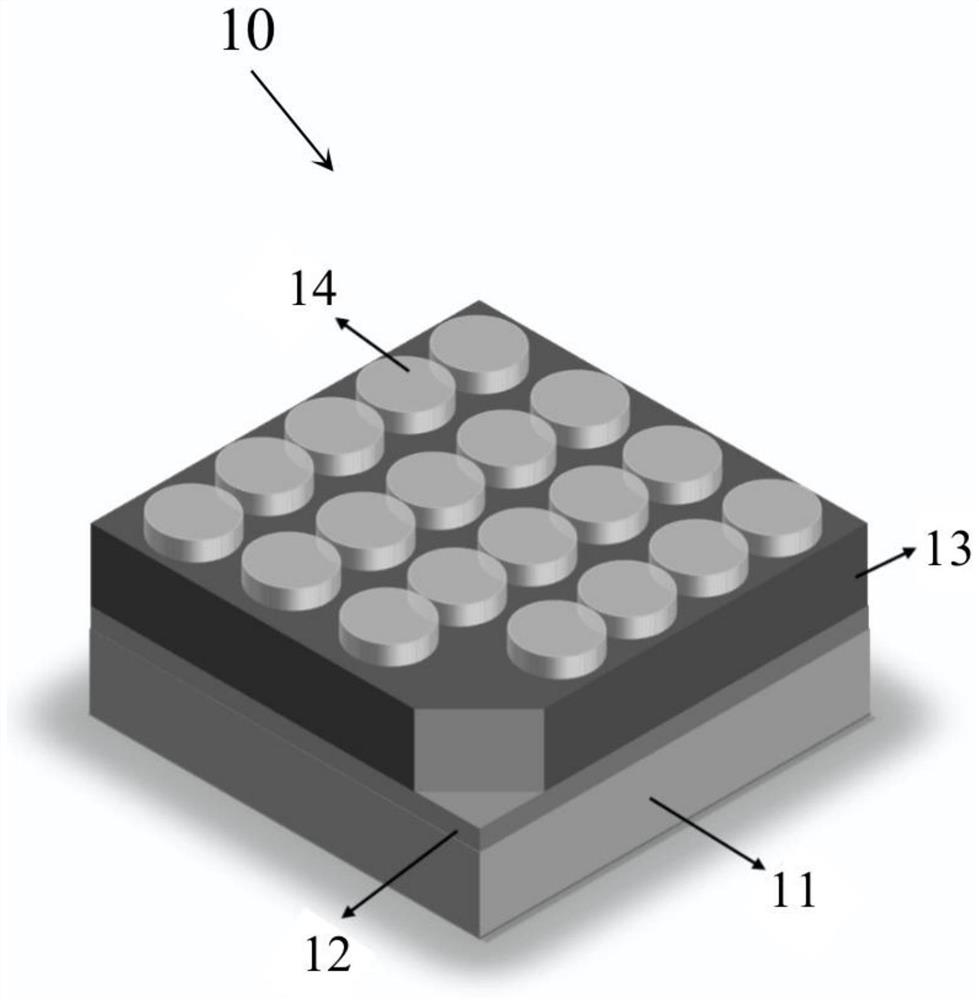
[0032] Such as figure 1 As shown, the RRAM 10 implementing multi-value storage provided in this embodiment includes a substrate 11 , a bottom electrode 12 , a dielectric layer 13 and a top electrode 14 arranged in sequence from bottom to top. Wherein the substrate 11 is a glass substrate, the bottom electrode 12 is an ITO film, and the dielectric layer 13 is copper antimony sulfur quantum dots (CuSbS 2 QDs) dielectric material, the top electrode 14 is an Au electrode.

[0033] Preparation:

[0034] (1) Select glass as the substrate 11, and deposit ITO on the surface of the substrate 11 by magnetron sputtering to form the bottom electrode 12; the sputtering power is 100W, and the d...


PUM


Abstract

The invention provides a dielectric layer for realizing multi-valued storage, a resistive random access memory and a preparation method and application of the resistive random access memory, CuSbS2 is used as a dielectric material of an RRAM (resistive random access memory), and the CuSbS2 can present bipolar and nonvolatile resistive characteristics and has relatively low switching voltage and high resistive switching ratio; meanwhile, lone pair electrons of Sb atoms and S3p are utilized to form a relatively high energy level of an anti-bond orbit to perform orbit hybridization with Sb 5p again, so that a new charge trapping state is formed, the dielectric layer and the resistive random access memory have the multi-valued storage performance, and the dielectric layer and the resistive random access memory with a novel multi-valued storage mechanism different from the prior art are obtained; and brand new application of the CuSbS2 in the field of memories is obtained. The resistive random access memory is characterized in that the dielectric layer is made of a CuSbS2 material. The preparation method is characterized in that a CuSbS2 material is adopted to form the dielectric layer. The dielectric layer is characterized in that a CuSbS2 material is adopted.

Description

technical field [0001] The invention belongs to the technical field of semiconductor manufacturing, and in particular relates to a medium layer for realizing multi-value storage, a resistive variable memory, a preparation method and application thereof. Background technique [0002] Resistive Switching Random Access Memory (RRAM) has been highly valued and extensively researched in academic and industrial fields because of its low cost, low energy consumption and excellent data storage characteristics, and it can become the biggest advantage of the next generation of non-volatile memory The reason is that RRAM has great potential for miniaturization. The purpose of the miniaturization of RRAM devices is to obtain high-density memory. The resistance transition mechanism of RRAM ensures that it can work normally in a unit device with a size of only a few nanometers, but even if the resistance transition mechanism of RRAM supports the continuous reduction of device size , The ...

Claims


Application Information

Patent Timeline
Patent Type & Authority Applications(China)
IPC IPC(8): H01L45/00C23C14/06C23C14/35
CPCC23C14/35C23C14/0623H10N70/8822H10N70/026
Inventor 周静王志青王雯雯陈文胡洋李昂吕承睿刘曰利
Owner WUHAN UNIV OF TECH
Why Eureka
Try Eureka