Organic light emitting device
A technology of organic light-emitting devices and light-emitting layers, which is applied in the manufacture of electric solid-state devices, semiconductor devices, semiconductor/solid-state devices, etc., can solve the problems of material loss and difficulty in manufacturing devices with large areas, and achieve high service life characteristics and low The effect of driving voltage and high efficiency
- Summary
- Abstract
- Description
- Claims
- Application Information
AI Technical Summary
Problems solved by technology
Method used
Image

Examples
Embodiment approach
[0394] According to an exemplary embodiment of the present invention, A is represented by the following Chemical Formula A-1.
[0395] [Chemical formula A-1]
[0396]
[0397] In Chemical Formula A-1,
[0398] Ar1 is substituted or unsubstituted aryl or deuterated aryl,
[0399] Ar2 is substituted or unsubstituted aryl or deuterated aryl,
[0400] T is selected from a direct bond; substituted or unsubstituted aryl; and deuterated aryl, and
[0401] * indicates the point of incorporation in the copolymer.
[0402] In an exemplary embodiment of the present invention, A is represented by the following Chemical Formula A-2.
[0403] [Chemical formula A-2]
[0404]
[0405] In Chemical Formula A-2,
[0406] Ar1 is each independently substituted or unsubstituted aryl or deuterated aryl,
[0407] Ar each independently is a substituted or unsubstituted aryl or deuterated aryl,
[0408] Ar3 is substituted or unsubstituted aryl or deuterated aryl,
[0409] q is an integer...
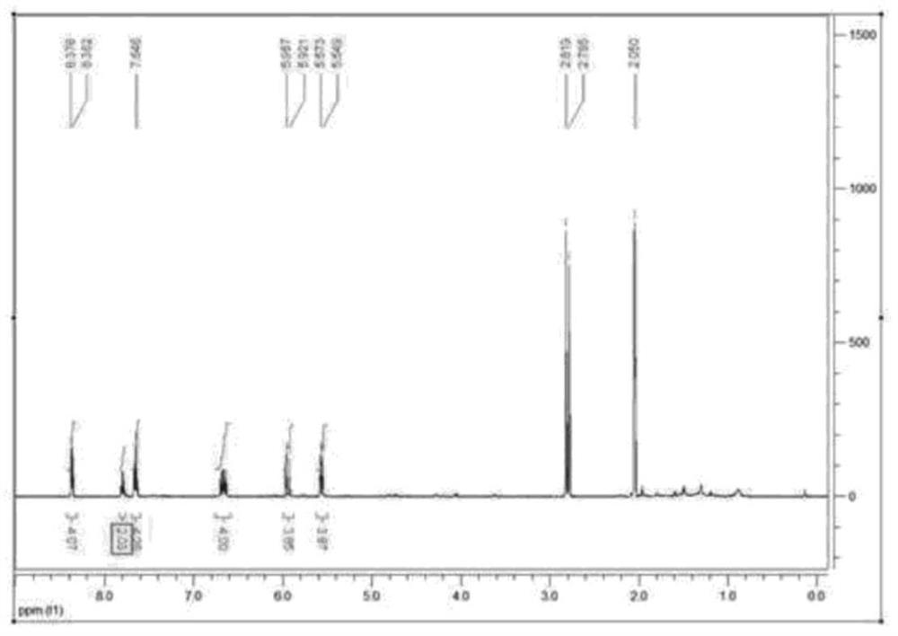
preparation example 1
[0732] Preparation Example 1. Synthesis of Compound A
[0733]
[0734] Synthesis of A-Int: Put diiodobiphenyl (10.0 g, 24.6 mmol), 4-fluoroaniline (5.12 mL, 54.2 mmol) and sodium tert-butoxide [hereinafter referred to as NaOtBu] (7.10 g, 73.9 mmol) into a round bottom flask (RBF), then introduced toluene (120 mL) therein. Introducing Pd( t Bu 3 P) 2 (0.629 g, 1.23 mmol), the resulting mixture was stirred at 90° C. for 1 hour. Thereafter, water was added thereto, and the organic layer was extracted with ethyl acetate (EA), followed by MgSO 4 It was dried, put dichloromethane (DCM) in it, and the resulting mixture was filtered to obtain A-Int (6.10 g).
[0735] Synthesis of A: A-Int (1.50g, 4.03mmol), L1 (4.83g, 8.46mmol) and NaOtBu (1.16g, 12.1mmol) were put into a round bottom flask (RBF), and toluene (30mL ). After heating the resulting mixture to 90 °C, Pd ( t Bu 3 P) 2 (0.144 g, 0.282 mmol), and the resulting mixture was stirred for 1 hour. Water was added th...
preparation example 2
[0737] Preparation Example 2. Synthesis of Compound B
[0738]
[0739] Synthesis of B-Int: Diiodobiphenyl (12.0 g, 29.6 mmol), 3,4-difluoroaniline (6.45 mL, 65.0 mmol) and NaOtBu (8.52 g, 88.7 mmol) were placed in a round bottom flask (RBF) , and toluene (150 mL) was then introduced therein. Introducing Pd( t Bu 3 P) 2 (0.755 g, 1.48 mmol), the resulting mixture was stirred at 90° C. for 1 hour. Thereafter, water was added thereto, and the organic layer was extracted with ethyl acetate (EA), followed by MgSO 4 It was dried, put dichloromethane (DCM) in it, and the resulting mixture was filtered to obtain B-Int (9.56 g).
[0740] Synthesis of B: B-Int (0.600g, 1.47mmol), L1 (1.70g, 2.98mmol) and NaOtBu (0.424g, 4.41mmol) were put into a round bottom flask (RBF), and toluene (20mL ). After heating the resulting mixture to 90 °C, Pd ( t Bu 3 P) 2 (0.0526 g, 0.103 mmol), and the resulting mixture was stirred for 1 hour. Water was added thereto, and the organic layer...
PUM
| Property | Measurement | Unit |
|---|---|---|
| boiling point | aaaaa | aaaaa |
| thickness | aaaaa | aaaaa |
| thickness | aaaaa | aaaaa |
Abstract
Description
Claims
Application Information