Organic light emitting device with low refractive capping layer

A technology for organic light-emitting devices and covering layers, which is applied to organic light-emitting devices, organic light-emitting device parameters, organic semiconductor devices, etc. The effect of current efficiency

Pending Publication Date: 2022-03-18
PNH TECH
View PDF0 Cites 0 Cited by
  • Summary
  • Abstract
  • Description
  • Claims
  • Application Information

AI Technical Summary

Problems solved by technology

[0004] The light efficiency of organic light-emitting devices can usually be divided into internal quantum efficiency (Internal quantum efficiency) and external quantum efficiency (external quantum efficiency). It is related to the generation of excitons in the organic layer between the cathodes and the light conversion efficiency. On the other hand, the external quantum efficiency refers to the efficiency at which the light generated in the organic layer is extracted to the outside of the organic light-emitting device (internal quantum efficiency × light extraction efficiency) , even if a high light conversion efficiency is achieved in the organic layer inside the device, if the external quantum efficiency according to the light extraction efficiency (Light coupling efficiency) is low, the overall light efficiency of the organic light-emitting device inevitably decreases

Method used


Image

  • Organic light emitting device with low refractive capping layer
  • Organic light emitting device with low refractive capping layer
  • Organic light emitting device with low refractive capping layer

Examples


Embodiment 1 to 2

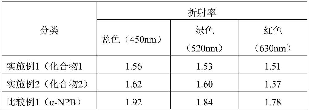
[0061] On the glass substrate, the covering layer compounds 1 and 2 for realizing the organic light-emitting device of the present invention were respectively deposited for 60-100 nm to measure the refractive index.

[0062] Quartz glass / organic (60~100nm)

experiment example 1

[0065] Experimental Example 1: Optical Characteristics of Experimental Examples 1 to 2

[0066] The refractive index of the substrate manufactured according to the above-mentioned examples was measured by ellipsometry (Ellipsometry, Elli-SE). The refractive index was measured in each wavelength region of blue (450 nm), green (520 nm), and red (630 nm), and the results are shown in Table 1 below.

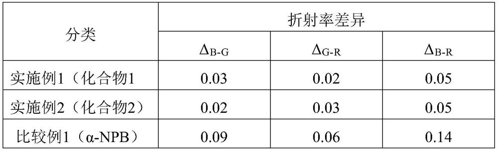
[0067] And, the refractive index difference (Δ B-G : difference between the refractive index of the blue (450nm) wavelength region and the refractive index of the green (520nm) wavelength region; Δ G-R : The difference between the refractive index in the green (520nm) wavelength region and the refractive index in the red (630nm) wavelength region; Δ B-R : the difference between the refractive index in the blue (450nm) wavelength region and the refractive index in the red (630nm) wavelength region), and is shown in Table 2 below.

[0068] Finally, the refractive indices in the wave...

Embodiment 3 to 4

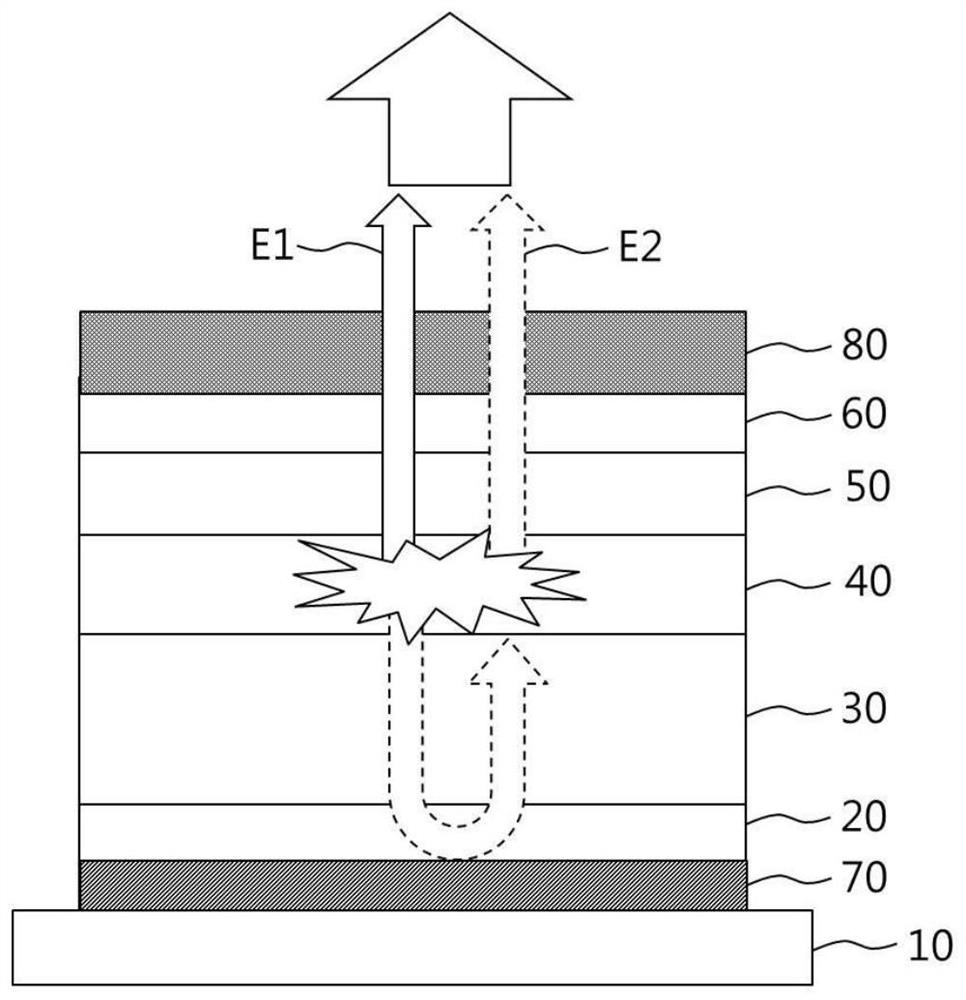
[0080] An organic light-emitting device having the following structure having a capping layer satisfying the specified conditions of the present invention was manufactured, and light-emitting characteristics including light-emitting efficiency were measured.

[0081] Ag / ITO / hole injection layer (HAT-CN, 5nm) / hole transport layer (TAPC, 100nm) / electron blocking layer (TCTA, 10nm) / light emitting layer (20nm) / electron transport layer 201 (Liq, 30nm) / LiF(1nm) / Mg:Ag(15nm) / Cover layer(70nm)

[0082] In order to form a hole injection layer on an Ag-containing ITO transparent electrode on a glass substrate, a HAT-CN film was formed to a thickness of 5 nm, and then a TAPC film was formed to a thickness of 100 nm as a hole transport layer. A TCTA film was formed with a thickness of 10 nm as an electron blocking layer. And, a light-emitting layer was co-deposited at 20 nm using BH1 as a host compound and BD1 as a dopant compound. Further, an electron transport layer (doped with the fo...


PUM

PropertyMeasurementUnit
Thicknessaaaaaaaaaa
Peak wavelengthaaaaaaaaaa
Bandgapaaaaaaaaaa

Abstract

The present invention relates to an organic light-emitting device having a low refractive index capping layer, thereby improving light extraction efficiency, reducing driving voltage, improving power efficiency, and improving current efficiency at the same time.

Description

technical field [0001] The present invention relates to an organic light emitting device, and in more detail, to an organic light emitting device having a capping layer with a low refractive index, thereby improving light extraction efficiency, further reducing driving voltage, and improving current efficiency. Background technique [0002] An organic light emitting diode is a self-luminous device, which has the advantages of wide viewing angle, excellent contrast, short response time, excellent brightness, driving voltage and response speed characteristics, and can realize multi-color. [0003] The driving and light-emitting principle of this organic light-emitting device is as follows: When a voltage is applied between the anode and the cathode, the holes injected from the anode move to the light-emitting layer through the hole transport layer, and the electrons injected from the cathode move to the light-emitting layer through the electron transport layer. The light-emitt...

Claims


Application Information

Patent Timeline
IPC IPC(8): H01L51/52H01L51/50H01L51/56
CPCH10K50/11H10K2101/10H10K50/858H10K71/00H10K50/828H10K2102/351H10K50/13H10K2101/00
Inventor 玄瑞镕尹石根尹度烈高恩志
Owner PNH TECH
Why Eureka
Try Eureka