Micro OLED display structure and preparation method thereof
A technology for displaying structure and functional layer, applied in the field of display screen, can solve the problems of optical crosstalk, affecting display effect, color crosstalk, etc., and achieve the effect of good application prospect, reduction of optical crosstalk, and simple structure
- Summary
- Abstract
- Description
- Claims
- Application Information
AI Technical Summary
Problems solved by technology
Method used
Image


Examples
Embodiment Construction
[0022] The specific implementation manner of the present invention will be described in further detail below by describing the embodiments with reference to the accompanying drawings.
[0023] In the description of the present invention, it should be noted that the terms "upper", "lower", "front", "rear", "left", "right", "vertical", "inner", "outer" etc. The indicated orientation or positional relationship is based on the orientation or positional relationship shown in the drawings, and is only for the convenience of describing the present invention and simplifying the description, rather than indicating or implying that the referred device or element must have a specific orientation, or in a specific orientation. construction and operation, therefore, should not be construed as limiting the invention.
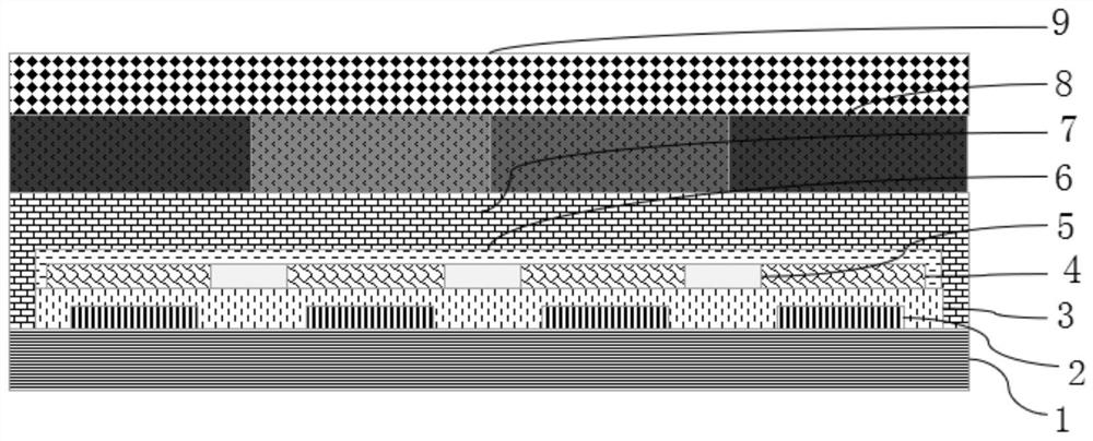
[0024] This Micro OLED display structure of the present invention, such as figure 1 As shown in , including a driving backplane 1, an anode 2 and a hole transport functional...
PUM
| Property | Measurement | Unit |
|---|---|---|
| thickness | aaaaa | aaaaa |
Abstract
Description
Claims
Application Information