Segmented bent and attached conductive insulation protection sheet

An insulating protection, segmented technology, used in film/sheet release liners, film/sheet adhesives, adhesives, etc., can solve problems such as the inability to meet the diverse needs of devices

Pending Publication Date: 2022-03-25
SUZHOU YIBANG ELECTRONICS MATERIAL CO LTD
0 Cites 0 Cited by

AI-Extracted Technical Summary

Problems solved by technology

However, the existing protective film is usually an integrated structure, which rarely achieves the integration of insulation and conductivity, and rar...

Method used

Conductive double-sided adhesive tape 7 adopts tesa60384 to make, has good electrical conductivity, and thickness is 100 μ m, and x-y direction surface resistance is 0.2 Ω/sq, and z direction contact resistance is 0.04 Ω/in 2 .
MYLAR adhesive tape II 6 adopts FTBFAP-15, comprises black polyester film, acrylic adhesive layer, release layer arranged successively from top to bottom, total thickness is 15-40 μ m, has better shading effect, 180 ° peeling machine The peeling force of the test is greater than 500g/25mm.
MYLAR adhesive tape II 6 adopts black FTBFAP-15, comprises black polyester film, acrylic adhesive layer, release layer arranged successively from top to bottom, total thickness...

Abstract

The invention discloses a sectional type bent and attached conductive insulation protection sheet which comprises a grid release film, an MYLAR adhesive tape I is arranged on one side of the grid release film, a silica gel protection film covers the grid release film and the MYLAR adhesive tape I at the same time, and a conductive insulation composite film is arranged between the silica gel protection film and the grid release film. In the invention, the MYLAR adhesive tape II, the front release film, the rear release film, the double-sided adhesive tape and the conductive double-sided adhesive tape are integrally connected, a gap is formed between the front release film and the rear release film, a gap is formed between the double-sided adhesive tape and the conductive double-sided adhesive tape, and the insulated double-sided adhesive tape and the conductive double-sided adhesive tape with conductivity are arranged below the MYLAR adhesive tape II. Through the MYLAR adhesive tape I, a plurality of conductive and insulating composite films with silica gel protective films can be compounded on the same grid release film, the adhesion force is enhanced, falling is not prone to occurring, the overall structure is suitable for being bent and attached, the double functions of conduction and insulation are achieved, and the overall structure is simple and suitable for industrial application and popularization.

Application Domain

Film/foil adhesive release liners

Technology Topic

Colloidal silicaSilicone tape +6

Image

  • Segmented bent and attached conductive insulation protection sheet
  • Segmented bent and attached conductive insulation protection sheet

Examples

  • Experimental program(1)

Example Embodiment

[0034] Example 1
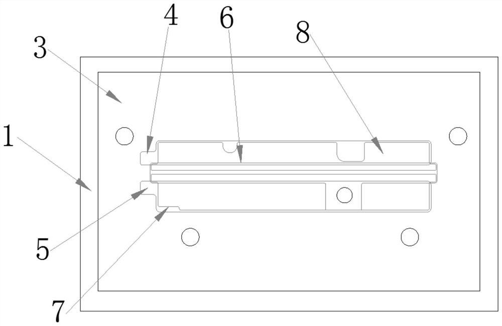
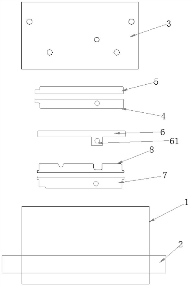
[0035] like Figure 1-2 As shown in the figure, a segmented bending and attaching conductive insulating protective sheet includes a grid release film 1, one side of the grid release film 1 is provided with MYLAR tape Ⅰ2 along its length direction, and a silicone protective film 3 covers it. On the grid release film 1 and MYLAR tape I2, a part of the silicone protective film 3 is directly bonded to the MYLAR tape I2, and the rest of the silicone protective film 3 is directly bonded to the grid release film 1 with a Conductive and insulating composite film, the size of the conductive and insulating composite film is smaller than the size of the silica gel protective film 3 bonded on the grid release film 1 . A number of conductive and insulating composite films can be bonded on the grid release film 1 through MYLAR tape I2.
[0036] The conductive and insulating composite film includes a front release film 4 and a rear release film 5, MYLAR tape II 6, and a conductive double-sided adhesive 7 and Double-sided adhesive 8, conductive double-sided adhesive 7 in the front, double-sided adhesive 8 in the back, the front release film 4 and the rear release film 5 are arranged at intervals, and there is a gap between the two opposite surfaces, which can be torn off in stages The front release film 4 and the rear release film 5 do not affect each other. The conductive double-sided adhesive 7 and the double-sided adhesive 8 are arranged at intervals. There is a distance between the two opposite surfaces. The front release film 4 and the rear release film The gap between 5 is adapted to the gap between the conductive double-sided adhesive 7 and the double-sided adhesive 8. More specifically, part of the bottom surface of the front release film 4 and the rear release film 5 are respectively bonded to the front and rear sides of the top of the MYLAR tape II 6, and then the front release film 4 and the rear release film 5 are integrated using the MYLAR tape II 6. The conductive double-sided adhesive 7 and the top part of the double-sided adhesive 8 are respectively bonded to the front and rear sides of the bottom of the MYLAR tape Ⅱ6, and then the conductive double-sided adhesive 7 and the double-sided adhesive 8 are connected together by using the MYLAR tape Ⅱ6. The conductive double-sided adhesive Both sides of 7 and double-sided adhesive tape 8 are sticky, and can adhere to front release film 4, rear release film 5, MYLAR tape II 6, and MYLAR tape II 6 plays the role of bonding and insulation.
[0037] Grid release film 1 adopts transparent LDW36T105 release film, including release layer, diamond-shaped PE layer, PET, PE and anti-adsorption layer arranged in sequence from top to bottom, with a total thickness of 90 μm and a width of 1040 mm, 180° peeling machine The release force of the test is 3g/25mm.
[0038] MYLAR tape Ⅰ 2 adopts SDK2296CR, the total thickness is controlled at 60μm, and the color is red, which is easy to identify and avoid missing stickers.
[0039] Silicone protective film 3 is made of transparent S7512L-38, with polyester film PET as the base material. The polyester film PET has two layers. The polyester film PET is coated with a silicone glue layer, and the silicone glue layer faces away from the polyester film PET. One side is laminated with a layer of polyester film PET, the sum of the thickness of the two layers of polyester film PET is 0.076mm, the thickness of a single layer of polyester film PET is 0.038mm, and the thickness of the silicone glue layer is 0.01mm, 180° peeling machine The peel force of the test is 12.5g/25mm, the test standard is GB/T2792-1998, the sample test width is 25mm, the test object is SUS304 steel plate, the test speed is 300mm/min, the test conditions are: temperature 23±2℃, Relative humidity 65±5%. Several through holes of circular structure are opened on the silica gel protective film 3 .
[0040] The front release film 4 and the rear release film 5 are made of blue 100T055B respectively, the thickness of the front release film 4 and the rear release film 5 are respectively 0.1mm, and the residual adhesion rate tested by a 5000g range tensile machine is not less than 85% %, the peeling force tested by a 180°5000g range tensile machine is 25g/25mm. The front release film 4 is bonded to the grid release film 1 through the viscosity of MYLAR tape Ⅱ6 and the conductive double-sided adhesive 7, and the rear release film 5 is bonded to the grid through the viscosity of MYLAR tape Ⅱ6 and double-sided adhesive 8. grid release film 1. The left ends of the front release film 4 and the rear release film 5 respectively offer a step-structure avoidance port. Offer circular through holes on the front release film 4 .
[0041] MYLAR tape Ⅱ6 adopts black FTBFAP-15, including black polyester film, acrylic adhesive layer, and release layer arranged in sequence from top to bottom, with a total thickness of 15 μm, which has a good light-shielding effect and is peeled off by a 180° peeling machine test. The force is greater than 500g/25mm.
[0042] As a more specific embodiment, the front side of the MYLAR adhesive tape II 6 is provided with a square or other structure of protrusions 61 , and a circular or other structure of escape openings are provided on the protrusions 61 .
[0043] Conductive double-sided adhesive 7 is made of tesa60384, which has good conductivity, the thickness is 100μm, the surface resistance in the x-y direction is 0.2Ω/sq, and the contact resistance in the z direction is 0.04Ω/in 2.
[0044] The double-sided adhesive tape 8 is made of transparent tesa4982 with a thickness of 100 μm and an elongation at break of 45%.
[0045] The left ends of the conductive double-sided adhesive tape 7 and the double-sided adhesive tape 8 are provided with step-structure avoidance openings respectively. Offer circular through-holes on the conductive double-sided adhesive tape 7 . Offer several position-avoiding grooves on the double-sided adhesive tape 8 .
[0046] Parts or structures that are not described in detail in the present invention can use existing technologies, and will not be repeated here.

PUM

no PUM

Description & Claims & Application Information

We can also present the details of the Description, Claims and Application information to help users get a comprehensive understanding of the technical details of the patent, such as background art, summary of invention, brief description of drawings, description of embodiments, and other original content. On the other hand, users can also determine the specific scope of protection of the technology through the list of claims; as well as understand the changes in the life cycle of the technology with the presentation of the patent timeline. Login to view more.
Why Eureka
Try Eureka