Multi-color electrochromic structure and device with high brightness, saturation and purity and manufacturing method of multi-color electrochromic structure and device

An electrochromic layer and saturation technology, which is applied in the field of optics or optoelectronics, can solve problems such as the need to improve brightness, small color gamut, and low color saturation of colorful films, and achieve brilliant colors, stable colors, and high manufacturability Effect

Pending Publication Date: 2022-03-29
SUZHOU INST OF NANO TECH & NANO BIONICS CHINESE ACEDEMY OF SCI
View PDF0 Cites 0 Cited by
  • Summary
  • Abstract
  • Description
  • Claims
  • Application Information

AI Technical Summary

Problems solved by technology

But so far, the color saturation of colorful films is not high, or the brightness needs to be improved, or the color gamut is small. The application of this kind of structural color is difficult to meet the needs of the public.

Method used


Image

  • Multi-color electrochromic structure and device with high brightness, saturation and purity and manufacturing method of multi-color electrochromic structure and device
  • Multi-color electrochromic structure and device with high brightness, saturation and purity and manufacturing method of multi-color electrochromic structure and device
  • Multi-color electrochromic structure and device with high brightness, saturation and purity and manufacturing method of multi-color electrochromic structure and device

Examples


preparation example Construction

[0102] In some embodiments, the preparation method of the colorful electrochromic structure includes: by physical or chemical deposition, such as coating, printing, casting film, etc. or magnetron sputtering, electron beam evaporation, heat evaporation, electrochemistry Deposition, chemical vapor deposition, atomic force deposition, sol gel technique, etc. form the first optical structural layer or the second optical structure layer, a dielectric layer, or the like, and is not limited thereto.

[0103] Further, the preparation method of the colorful electrochromic structure includes:

[0104] A substrate is provided; a method of depositing a first optical structural layer or a second optical structuring layer is deposited on the substrate, and a medium layer is deposited on the first optical structural layer or a second optical structure layer; Different layers are deposited according to requirements.

[0105] Further, the method of deposition of the PVD includes thermal sanding, ...

Embodiment 1

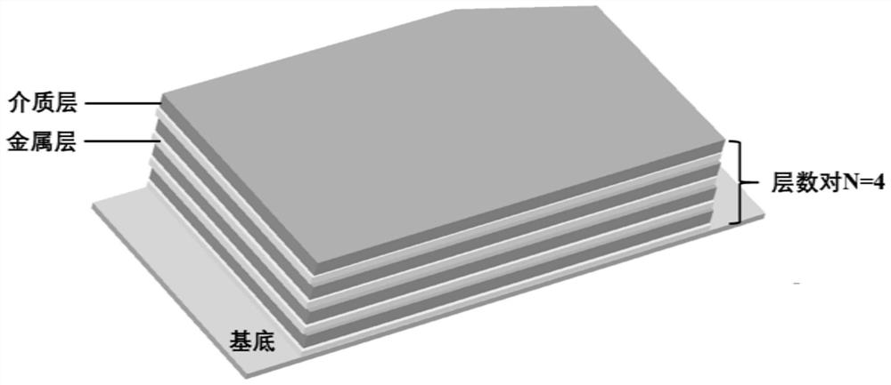
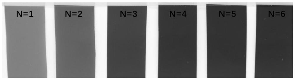
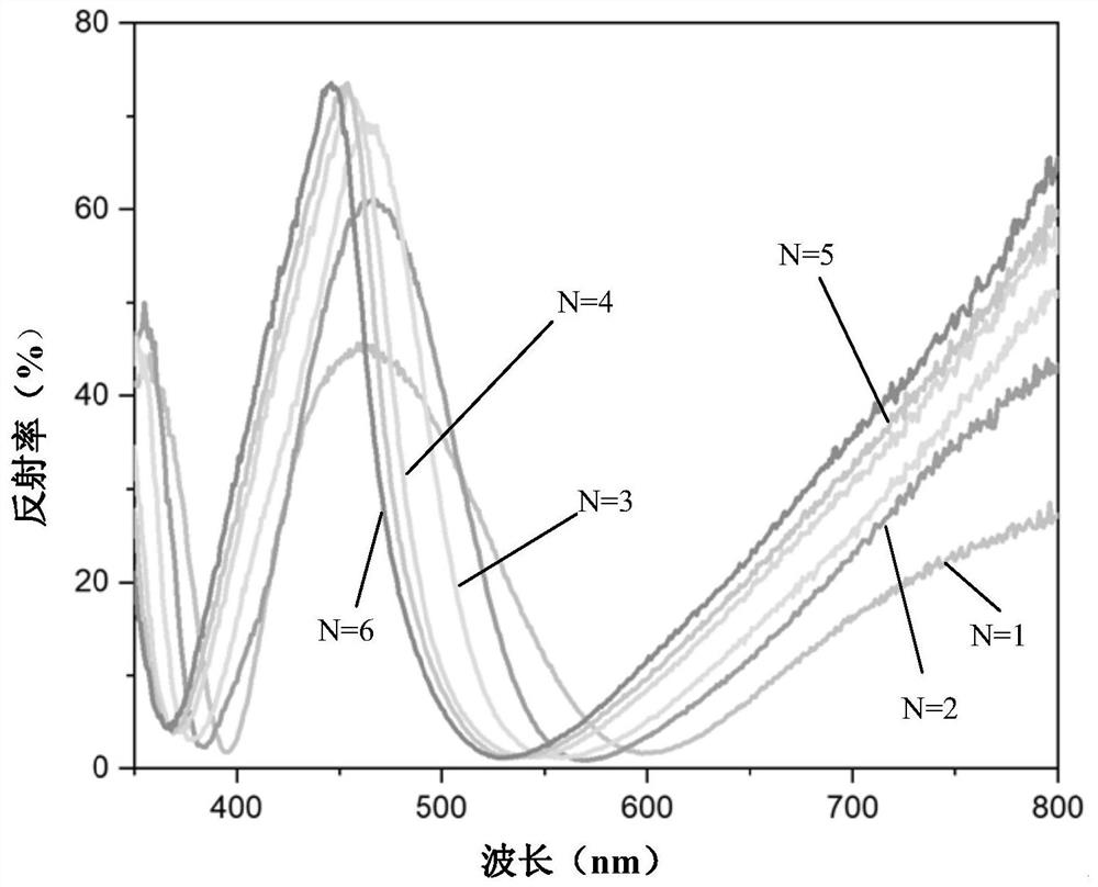
[0155] The preparation process of a multicolor, saturation, and purity of the present embodiment (may also be referred to as a colorful film) is as follows: in a clean PET substrate, a method of magnetron sputtering is deposited Layer W layer, thickness of about 10 ~ 30 nm; again in metal W layer, magnetron sputter one layer WO 3 The layer, the thickness is about 150 to 250 nm; the number of cycles can be obtained according to different requirements, and a colorful film of different layers to N = 2 to 6 (principle N ≥ 2) can be obtained. See figure 1As shown, the multicolored electrochromic film of the present embodiment includes a substrate, a metal layer, a dielectric layer, a metal layer, and a dielectric layer, which constitutes a metal-dielectric structure, which can generate optical multilayer film interference, thereby displaying colourful. figure 2 The real map of the colorful film is shown.

[0156] Of course, the aforementioned metal W layer can also be prepared using an...

Embodiment 2

[0160] The preparation process of a multi-color electrochromic film of the present embodiment disclosed is as follows: In the clean glass substrate, the desired pattern is obtained using a mask, and a layer is deposited by magnetron sputtering. The metal W layer, the thickness is about 10 ~ 30 nm; then the magnetron sputtering of the metal W layer is first WO 3 The layer, the thickness is about 150 to 250 nm; the number of cycles can be obtained according to different requirements, and a colorful film of different layers to N = 2 to 6 (principle N ≥ 2) can be obtained.

[0161] Of course, the aforementioned metal W layer can also be prepared using an electron beam evaporation, thermal plating. WO 3 The layer can be prepared by electron beam evaporation, thermurally plating, electrochemical deposition, and the like.


PUM

PropertyMeasurementUnit
thicknessaaaaaaaaaa
thicknessaaaaaaaaaa
thicknessaaaaaaaaaa

Abstract

The invention discloses a multi-color electrochromic structure with high brightness, saturation and purity, a device and a manufacturing method. The multi-color electrochromism structure comprises an electrochromism layer which comprises a plurality of layer-pair structures formed by sequentially and alternately stacking and arranging first optical structure layers or second optical structure layers and dielectric layers; the bonding interfaces of the dielectric layer and the first optical structure layer and the second optical structure layer are a first surface and a second surface of the dielectric layer respectively, and the first surface and the second surface are matched with the dielectric layer to form an optical cavity. The invention further discloses a multi-color electrochromic device. According to the invention, the metal layers with different thicknesses or the dielectric layers with different thicknesses are deposited on different substrates to serve as the electrochromic structure, so that a multi-color electrochromic structure with different brightness, saturation and purity can be realized. The multi-color electrochromic structure belongs to a structural color, is stable in color, gorgeous in color and high in manufacturing degree, and does not age or lose color after being exposed to an outdoor environment for a long time.

Description

Technical field [0001] The present invention relates to a colorful film comprising a colorful electrochromic structure of high brightness, saturation, purity, a preparation method thereof, and a corresponding colorful electrochromic device, belonging to optical or photoelectric technology. Background technique [0002] Electrochromosis is the optical property of the material in the application of circulating reversible changes under the voltage. For the most commonly used smart window, the electrochromic material device only needs to satisfy the modulation of light transparency, and in the application field of display devices, electrical Charloration is dynamic regulation of different colors by voltage. Colorful discoloration shows that before and after discoloration, the material exhibits a different color, which has strong appeal in the field of display devices and smart apparel. Colorful electrochromic techniques are mainly mainly organic small molecules or conjugated polymer ...

Claims


Application Information

Patent Timeline
Patent Type & Authority Applications(China)
IPC IPC(8): G02F1/157
CPCG02F1/157H01B5/14G02F1/153
Inventor 赵志刚武琦丛杉
Owner SUZHOU INST OF NANO TECH & NANO BIONICS CHINESE ACEDEMY OF SCI
Why Eureka
Try Eureka