Diffractive optical chip

A diffractive optics and chip technology, applied in diffraction gratings and other directions, can solve the problems of large surface shape combination, weakened energy of coated Gaussian mirror, complex aspheric surface shaping, etc., and achieves high device reliability, high integration and small volume. Effect

Pending Publication Date: 2022-04-08
HUAZHONG PHOTOELECTRIC TECH INST (CHINA SHIPBUILDING IND CORP THE NO 717 INST)
View PDF0 Cites 0 Cited by
  • Summary
  • Abstract
  • Description
  • Claims
  • Application Information

AI Technical Summary

Problems solved by technology

[0007] The present invention aims at the shortcomings of the above-mentioned prior art, and provides a diffractive optical chip, which is used to shape the Raman beam into a flat-hat beam with uniform intensity and phase, so as to improve the energy weakening of the current coated Gaussian mirror in the prior art. , aspherical shaping and combination of complex surface shapes and large optical path volume and other technical issues

Method used


Image

  • Diffractive optical chip
  • Diffractive optical chip
  • Diffractive optical chip

Examples


Embodiment Construction

[0041] The present invention will be described in further detail below in conjunction with the accompanying drawings.

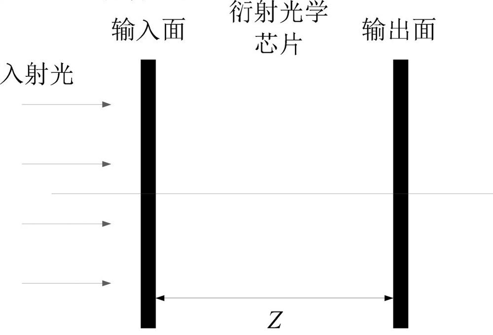
[0042] refer to figure 1 As shown, a diffractive optical chip disclosed in the present invention has an incident surface for intensity homogenization and an exit surface for phase homogenization, the micro-nano structures on the incident surface and the exit surface are centrosymmetric structures, The output surface can be round or square, or other shapes can be determined according to actual needs. The area of ​​the micro-nano structure on both sides can be made according to the diameter of the light source after collimation. The structure area of ​​the incident surface on the left side of this embodiment is 5.8 μm 2 ~20mm 2 , the structural area of ​​the exit surface on the right is 3.8 μm 2 ~ 20mm 2 , not limited to this area, the production area can be increased according to the needs, and the micro-nano structure area of ​​the two surfaces can be equ...


PUM

PropertyMeasurementUnit
thicknessaaaaaaaaaa
areaaaaaaaaaaa
areaaaaaaaaaaa

Abstract

The invention discloses a diffractive optical chip, which is provided with an incident surface for realizing intensity homogenization and an emergent surface for realizing phase homogenization, the outer diameters of the incident surface and the emergent surface are 25.4 mm, and the incident surface and the emergent surface are symmetrically arranged; fused quartz (JGS1) is used as a substrate material, a laser direct writing gray mask technology is adopted for continuous face type manufacturing, a micro-nano double-face monomer structure or a micro-nano four-face double-body structure with the thickness being 40 mm is formed, and the micro-nano four-face double-body structure further comprises two unstructured planes with the distance being 38 mm. The embodiment of the invention is simple in structure, ingenious in design and convenient to implement, has outstanding substantive features and remarkable progress, and is suitable for large-scale popularization and application.

Description

technical field [0001] The invention belongs to the technical field of beam shaping, and in particular relates to a diffractive optical chip, which is used to shape a Raman beam into a flat-hat beam. Background technique [0002] The traditional Raman light is a Gaussian beam. Because Raman light has intensity distribution and phase distribution, the spatial position and size of the atomic group are also changing, so the Raman light intensity felt by the atom is different, and the Rabi frequency of the atom at different positions different. [0003] One is that the atomic transition probability and phase in the atomic group are inconsistent, which seriously affects the system output fringe contrast and phase noise. [0004] The second is that the atomic clusters continue to diffuse during the falling process, and the diameter of the atomic clusters becomes larger. When the three Raman pulses are applied, the intensity and phase of the Raman light felt are different, and sys...

Claims


Application Information

Patent Timeline
Patent Type & Authority Applications(China)
IPC IPC(8): G02B5/18
Inventor 王晨晟董亭亭吴新建王建波张意
Owner HUAZHONG PHOTOELECTRIC TECH INST (CHINA SHIPBUILDING IND CORP THE NO 717 INST)
Why Eureka
Try Eureka