Hole filling method of circuit board and manufacturing method of double-sided circuit board

A circuit board and double-sided technology, applied in the direction of multi-layer circuit manufacturing, electrical connection formation of printed components, etc., can solve the problems of difficult liquid exchange, complicated process, increased equipment investment and production cost, etc., to eliminate hidden dangers in quality and process The process is simple and the production quality is good

Pending Publication Date: 2022-04-15
深圳市鼎华芯泰科技有限公司
View PDF0 Cites 0 Cited by
  • Summary
  • Abstract
  • Description
  • Claims
  • Application Information

AI Technical Summary

Problems solved by technology

However, the characteristics of its material make its circuit board processing technology different from that of traditional PCB. The metallization of the substrate hole needs to vacuum sputter a layer of seed layer on the hole wall, and then fill the hole with electroplating to achieve good heat transfer effect and the connection of the circuit layer. This process requires a large investment in equipment and a complicated process, and the surface copper is thickened at the same time when the holes are plated, which is not conducive to the production of fine lines; thick surface copper will cause increased stress, increase substrate warpage, and even cause board breakage
[0003] The traditional hole plating process is to plate copper on the hole wall. With the increase of hole copper, the hole diameter becomes smaller and smaller, and the liquid exchange becomes more and more difficult. Because the potential of the hole copper is higher than that of the middle hole wall copper, the hole The mouth part is easy to be closed first, and the liquid medicine inside the hole is encapsulated by the copper at the hole, forming a "core" and causing quality problems
The industry usually adopts the pulse electroplating process to solve the problem of "core wrapping", which not only increases equipment investment and production costs, but also makes it difficult to eliminate the quality hidden danger of "core wrapping"

Method used


Image

  • Hole filling method of circuit board and manufacturing method of double-sided circuit board
  • Hole filling method of circuit board and manufacturing method of double-sided circuit board
  • Hole filling method of circuit board and manufacturing method of double-sided circuit board

Examples


Embodiment Construction

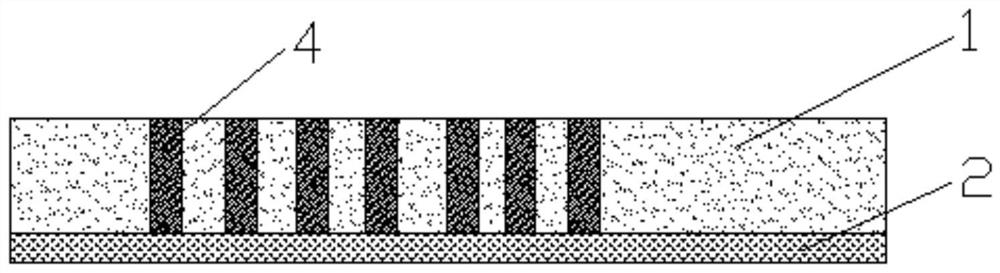
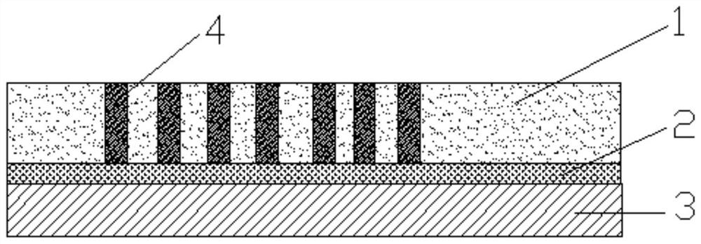
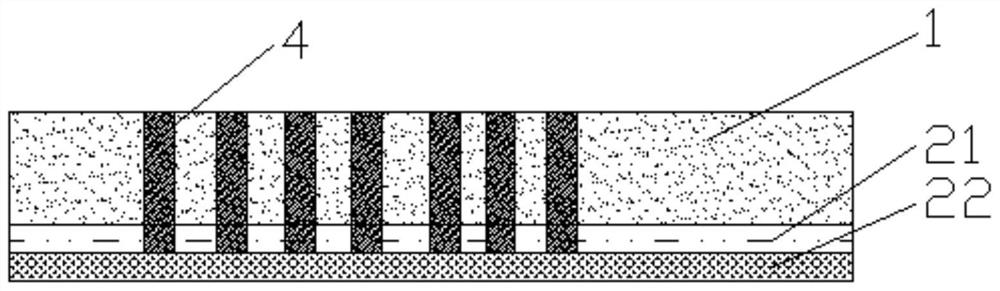
[0031] The hole filling method of the circuit board substrate in embodiment 1 of the present invention is as follows: figure 1 shown, including the following steps:

[0032] 101) Select the substrate 1, and perform laser drilling on the substrate 1. The position of the through hole is the overlapping area of ​​the circuit layer on the top surface of the circuit board and the circuit layer on the bottom surface;

[0033] 102) Covering the conductive adhesive layer 2 on the bottom surface of the substrate;

[0034] 103) electroplate the copper column 4 on the conductive adhesive layer 2 in the through hole, and the height of the copper column 4 is not less than the thickness of the substrate 1;

[0035] 104) Remove the conductive adhesive layer 2, and level the copper pillars higher than the opening on the top surface of the substrate 1.

[0036] The conductive adhesive layer 2 has good electrical conductivity and certain cohesiveness. It can be thermosetting adhesive or press...


PUM


Abstract

The invention discloses a hole filling method of a circuit board and a manufacturing method of a double-sided circuit board. The hole filling method comprises the following steps: punching a through hole in a substrate; pasting a conducting medium layer on one surface of the substrate; plating a copper column on the conductive dielectric layer in the through hole, so that the height of the copper column in the substrate is not less than the thickness of the substrate; and removing the conductive medium layer, and leveling the copper column higher than the orifice of the substrate. According to the invention, the hole wall does not need to be metallized, and the copper column is directly plated; the solid copper columns are arranged in the holes, so that the quality hidden danger of core wrapping is avoided; the technical process is simple, the hole filling efficiency is high, the quality is good, and the manufacturing quality of the double-sided circuit board is good.

Description

[technical field] [0001] The invention relates to a method for manufacturing a circuit board, in particular to a method for filling holes in a circuit board and a method for manufacturing a double-sided circuit board. [Background technique] [0002] Inorganic dielectric substrates such as ceramic substrates and glass substrates are widely used on printed circuit boards. However, the characteristics of its material make its circuit board processing technology different from that of traditional PCB. The metallization of the substrate hole needs to vacuum sputter a layer of seed layer on the hole wall, and then fill the hole with electroplating to achieve good heat transfer effect and the connection of the circuit layer. This process requires a large investment in equipment and a complicated process, and the surface copper is thickened at the same time when the holes are plated, which is not conducive to the production of fine lines; thick surface copper will cause increased st...

Claims


Application Information

Patent Timeline
Patent Type & Authority Applications(China)
IPC IPC(8): H05K3/42H05K3/46
Inventor 徐光泽沈正何忠亮
Owner 深圳市鼎华芯泰科技有限公司
Why Eureka
Try Eureka