Formation method of semiconductor structure

A semiconductor and pattern structure technology, which is applied in the fields of semiconductor devices, semiconductor/solid-state device manufacturing, and electric solid-state devices, etc., can solve the problems of increasing the difficulty and complexity of integrated circuits, and achieve high lithography process friendliness, small changes and small changes. The effect of key dimensions

Pending Publication Date: 2022-04-22
SEMICON MFG INT (SHANGHAI) CORP +1
View PDF0 Cites 0 Cited by
  • Summary
  • Abstract
  • Description
  • Claims
  • Application Information

AI Technical Summary

Problems solved by technology

[0003] During the development of integrated circuits, usually as the functional density (that is, the number of interconnection structures per chip) gradually increases, the geometric size (that is, the minimum component size that can be produced using process steps) also gradually decreases. Correspondingly increases the difficulty and complexity of integrated circuit manufacturing
[0004] At present, in the case of shrinking technology nodes, how to improve the matching degree between the pattern formed on the wafer and the target pattern has become a challenge

Method used


Image

  • Formation method of semiconductor structure
  • Formation method of semiconductor structure
  • Formation method of semiconductor structure

Examples


Embodiment Construction

[0021] It can be known from the background art that how to improve the matching degree between the pattern formed on the wafer and the target pattern becomes a challenge in the case of shrinking technology nodes.

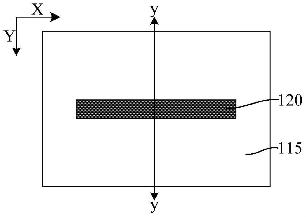
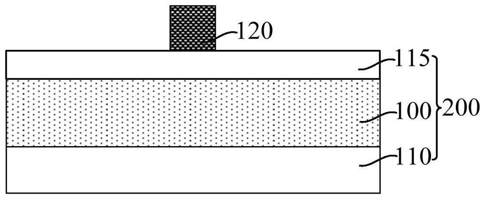
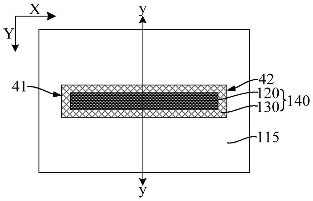
[0022] In order to solve the above technical problem, an embodiment of the present invention provides a method for forming a semiconductor structure, including: providing a substrate including a target layer for forming a target pattern; forming a core layer extending along a first direction on the substrate, The direction perpendicular to the first direction is the second direction; sidewalls are formed on the sidewalls of the core layer, and the core layer and the sidewalls located on the sidewalls of the core layer form a graphic structure layer; A sacrificial layer is formed on the substrate across the pattern structure layer along the second direction, and the sacrifice layer covers at least part of the top and part of the sidewall of the pattern structure layer...


PUM


Abstract

A method for forming a semiconductor structure comprises the following steps: providing a substrate which comprises a target layer for forming a target pattern; forming a core layer extending along a first direction on the substrate, wherein a direction perpendicular to the first direction is a second direction; forming a side wall on the side wall of the core layer, wherein the core layer and the side wall located on the side wall of the core layer form a graphic structure layer; forming a sacrificial layer crossing the graphic structure layer in the second direction on the substrate, wherein the sacrificial layer at least covers part of the top and part of the side wall of the graphic structure layer; forming a flat layer on the substrate exposed by the sacrificial layer and the graphic structure layer; the sacrificial layer is removed, first grooves are formed in the flat layer, and the first grooves are located in the two sides of the pattern structure layer; the core layer is removed, so that a second groove is defined by the side walls; and etching the target layer below the first groove and the second groove by taking the flat layer and the side wall as masks to form a target pattern. The embodiment of the invention is beneficial to further compressing the pitch between the target patterns.

Description

technical field [0001] Embodiments of the present invention relate to the field of semiconductor manufacturing, and in particular, to a method for forming a semiconductor structure. Background technique [0002] With the rapid growth of the semiconductor integrated circuit (Integrated circuit, IC) industry, semiconductor technology continues to move towards smaller process nodes driven by Moore's Law, making integrated circuits smaller in size, higher in circuit precision, and development in the direction of higher complexity. [0003] During the development of integrated circuits, usually as the functional density (that is, the number of interconnection structures per chip) gradually increases, the geometric size (that is, the minimum component size that can be produced using process steps) also gradually decreases. Correspondingly increases the difficulty and complexity of integrated circuit manufacturing. [0004] At present, how to improve the matching degree between t...

Claims


Application Information

Patent Timeline
Patent Type & Authority Applications(China)
IPC IPC(8): H01L21/768
CPCH01L21/76816H01L2221/101
Inventor 金吉松
Owner SEMICON MFG INT (SHANGHAI) CORP
Why Eureka
Try Eureka