

Soldering method of laser circuit board solder paste welding machine
A circuit board and soldering technology, applied in the direction of welding/welding/cutting items, welding equipment, manufacturing tools, etc., can solve the problems of complex production process, unsatisfactory comprehensive energy saving effect, unavoidable baking process of glue and glue curing, etc. , to achieve the effect of improving the yield rate, reducing frequent movement, and reducing system errors
- Summary
- Abstract
- Description
- Claims
- Application Information
AI Technical Summary
Problems solved by technology
Method used
Image

Examples
Embodiment 1
[0031] Embodiment 1: the concrete structure of the present invention is as follows:
[0032] Please refer to the attached Figure 1-3 , a soldering method of a laser circuit board solder paste soldering machine of the present invention, the soldering method comprises:
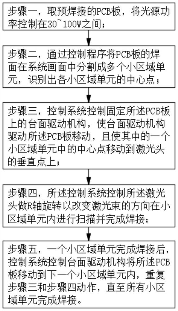
[0033] Step 1, take the pre-soldered PCB board, and control the power of the light source between 30 and 100W;
[0034] Step 2, divide the welding surface of the PCB board into a plurality of small area units in the system screen through the control program, and identify the center point of each small area unit;
[0035] Step 3, the control system controls and fixes the table driving mechanism on the PCB, so that the table driving mechanism drives the PCB to move, and moves the center point of one of the small area units to the vertical point of the laser head;
[0036] Step 4, the control system controls the laser head to rotate on the R axis to change the direction of the laser beam to scan in the small are...
Embodiment 2
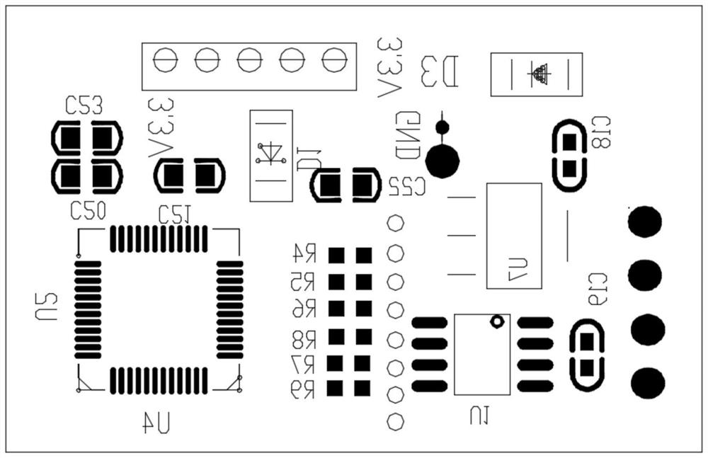
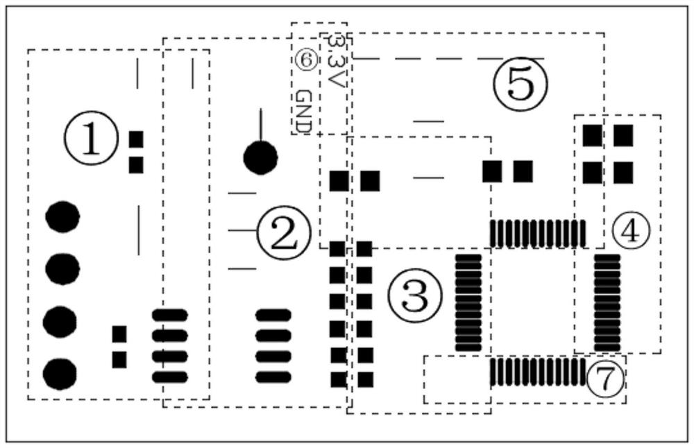
[0041] Such as Figure 1-10 , figure 1 It is a structural diagram of a pre-soldered PCB board with components in Example 2 of the present invention. figure 2 It is a distribution diagram of each small area unit of a pre-soldered PCB board soldering surface in Embodiment 2 of the present invention.
[0042] figure 2 Among them, the soldering surface of the PCB board is divided into 7 small area units, wherein the first small area unit 1 and the second small area unit 2 have an overlapping area, and the second small area unit 2 is respectively connected with the sixth small area unit 6 and the fifth small area unit. Unit 5 and the third small area unit 3 have an overlapping area, the sixth small area unit 6 and the fifth small area unit 5 have an overlapping area, the fifth small area unit 5 and the third small area unit 3 have an overlapping area, and the fifth small area unit 5 has an overlapping area. The area unit 5 and the fourth small area unit 4 have an overlapping a...
PUM
 Abstract
Description
Claims
Application Information