Device channel carrier average free path detection method and system

A detection method and detection system technology, applied in the field of semiconductor, can solve the problem of large mean free path error in measurement, and achieve the effect of accurate calculation value

Pending Publication Date: 2022-04-29
无锡芯鉴半导体技术有限公司
View PDF0 Cites 0 Cited by
  • Summary
  • Abstract
  • Description
  • Claims
  • Application Information

AI Technical Summary

Problems solved by technology

[0005] For this reason, the technical problem to be solved by the present invention is to

Method used


Image

  • Device channel carrier average free path detection method and system
  • Device channel carrier average free path detection method and system
  • Device channel carrier average free path detection method and system

Examples


Example Embodiment

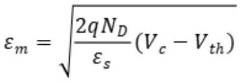
[0050] Based on the above embodiments, this embodiment is a specific embodiment of the device channel carrier average free path detection method, as follows:

[0051] In this embodiment, the average free path of the channel carrier of the detector at a constant temperature of room temperature 300K;

[0052] The utilization voltage range is the depletion region voltage and less than the cut-off voltage v th , the C-V curve is obtained by cyclic voltammetry simulation scanning, and 1 / C is obtained from the C-V curve 2 -V curve, through 1 / C 2 -Relation formula of V curve Obtain the donor concentration n D ;

[0053] Where q is the amount of electron charge, ε s Is the dielectric constant, Is the built-in potential, K is the Planck constant and t is the temperature;

[0054] A step bias voltage is applied to the device electrode by an ordinary voltage source or power source to obtain the critical voltage for generating hot spots;

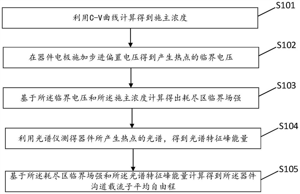
[0055] Calculate the critical field strength:

...


PUM


Abstract

The invention relates to a device channel carrier average free path detection method and system. The invention relates to a method for determining the average free path of carriers in a channel, which comprises the following steps of: calculating donor concentration by using a C-V curve, applying bias voltage to an electrode of a device to obtain critical voltage Vc generated by a hot spot, and solving critical field intensity of a depletion region based on the critical voltage Vc and the donor concentration ND; measuring an electroluminescent spectrum of a hot spot generated by the device by using a spectrograph, and calculating the characteristic peak energy of the spectrum; and solving the average free path of the carrier based on the critical field intensity of the depletion region and the spectral characteristic peak energy. According to the invention, the average free path of the carriers in the channel is determined by combining optical and electrical means, and the method is of great significance to research on physical characteristics of materials and devices.

Description

technical field [0001] The invention relates to the technical field of semiconductors, in particular to a device channel carrier mean free path detection method and system. Background technique [0002] In the existing technology, qualitatively speaking, the mean free path λ m is related to the carrier mobility μ, which is determined by the scattering mechanism, usually: [0003] [0004] Among them, v th is the thermal rate, τ m is the mean free time, k is the Boltzmann constant, K is the thermodynamic temperature, m* is the effective mass of the electron, and q is the charge of the electron. In traditional test schemes, the value of the mean free path is mostly determined by measuring the mobility. However, in the actual measurement process, there will be many errors, which will cause the calculated value of the mean free path to deviate from the theoretical value or the real value. In addition , in semiconductors, there are various scattering mechanisms of carriers...

Claims


Application Information

Patent Timeline
IPC IPC(8): G01R31/26G01N21/65
CPCG01R31/2603G01N21/65
Inventor 陈雷雷闫大为顾晓峰
Owner 无锡芯鉴半导体技术有限公司
Why Eureka
Try Eureka