Wafer optical film graphical processing efficient photoresist removing process method

A technology of optical film and process method, applied in the direction of photosensitive material processing, photoengraving process coating equipment, etc., can solve the problems of long time, difficult to remove glue, low efficiency, etc., and achieve the effect of improving processing efficiency and shortening the time of removing glue

Pending Publication Date: 2022-04-29
HANGZHOU MDK OPTO ELECTRONICS CO LTD
View PDF0 Cites 0 Cited by
  • Summary
  • Abstract
  • Description
  • Claims
  • Application Information

AI Technical Summary

Problems solved by technology

like figure 1 As shown, at present, the traditional wafer optical thin film patterning processing and removal process is the liftoff process, but because the optical film is blocked above the adhesive layer, the adhesive removal solution cannot directly contact the photoresist, and it is difficult to remove the adhesive. , long time and low efficiency

Method used


Image

  • Wafer optical film graphical processing efficient photoresist removing process method
  • Wafer optical film graphical processing efficient photoresist removing process method

Examples


Embodiment

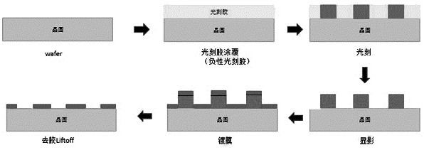
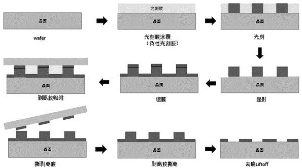
[0020] Example: as attached figure 2 As shown, a process method for patterning wafer optical film processing and efficient deglue, the steps of the process method are:

[0021] S1: select the wafer;

[0022] S2: Coating photoresist on the wafer by spin coating;

[0023] S3: Use the photolithography process to expose the photoresist, and the photoresist pattern depends on the Mask design; the photoresist in the pattern area illuminated by UV will form a substance that is not easily soluble in the developer solution, and will not be exposed to UV. The photoresist in the illuminated pattern area is easily soluble in the developer;

[0024] S4: Develop after photolithography, remove the photoresist in the pattern area that is easily soluble in the developer solution through the developer solution, and obtain a photoresist-patterned wafer;

[0025] S5: performing optical thin film deposition and coating on the photoresist patterned wafer to obtain a wafer after optical thin fil...


PUM


Abstract

The invention discloses an efficient photoresist removing process method for wafer optical thin film graphical processing. According to the method, the optical thin film deposited on the photoresist is removed by adopting a stripping adhesive tape pasting mode, and the exposed photoresist is directly contacted with the photoresist removing liquid in the photoresist removing process and is easier to remove, so that the photoresist removing time is greatly shortened, and the wafer optical thin film patterning processing efficiency is improved. The problems that in a traditional photoresist removing lift mode, due to blocking of an optical thin film above a photoresist layer, photoresist removing liquid cannot make direct contact with photoresist, photoresist removing is difficult, time is long, and efficiency is low are solved.

Description

technical field [0001] The invention belongs to the field of fabricating a patterned optical filter film on a wafer (wafer), and in particular relates to a process method for patterning processing of a wafer optical film with high efficiency and deglue. Background technique [0002] With the rapid development of miniaturization and integration of semiconductor chips, the size of the patterned optical film on the semiconductor wafer is also getting smaller and smaller. Such as figure 1 As shown, at present, the traditional wafer optical thin film patterning processing and removal process is the liftoff process, but because the optical film is blocked above the adhesive layer, the adhesive removal solution cannot directly contact the photoresist, and it is difficult to remove the adhesive. , long time and low efficiency. It is of great research significance to seek a way to quickly remove the optical film above the photoresist layer before removing the glue. Contents of ...

Claims


Application Information

Patent Timeline
Patent Type & Authority Applications(China)
IPC IPC(8): G03F7/30G03F7/16
CPCG03F7/30G03F7/16G03F7/162
Inventor 刘耀菊陈银培田双江邓宇杨巨椽
Owner HANGZHOU MDK OPTO ELECTRONICS CO LTD
Why Eureka
Try Eureka