Wafer-level fan-out packaging structure and preparation method thereof
A packaging structure, wafer-level technology, applied in semiconductor/solid-state device manufacturing, semiconductor/solid-state device components, semiconductor devices, etc. The effect of slice time
- Summary
- Abstract
- Description
- Claims
- Application Information
AI Technical Summary
Problems solved by technology
Method used
Image
Examples
no. 1 example
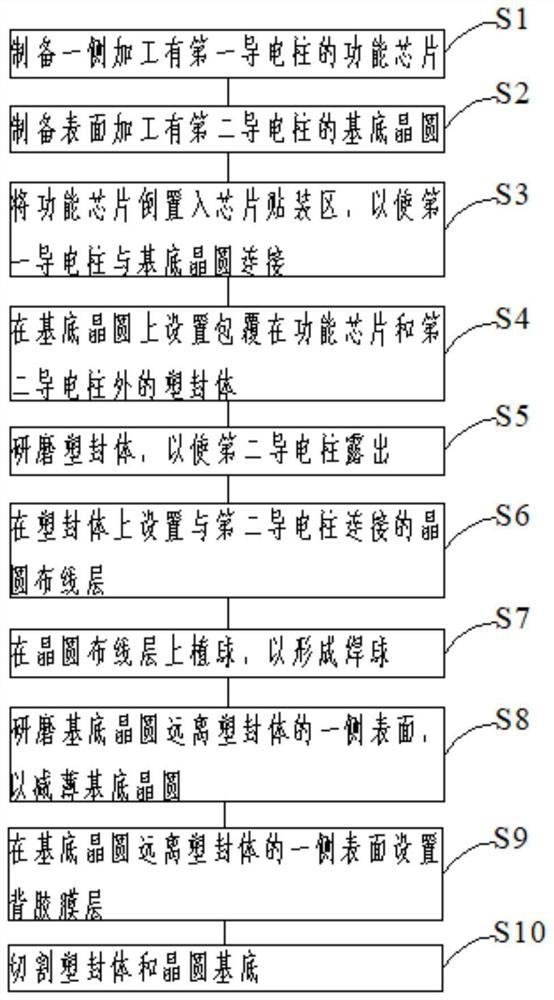
[0062] see figure 1 and Figure 10 , this embodiment provides a method for preparing a wafer-level fan-out packaging structure, which is used to prepare a wafer-level fan-out packaging structure 100, and the wafer-level fan-out packaging structure 100 is a fully encapsulated structure. The preparation method of the wafer-level fan-out packaging structure provided in the example can greatly reduce the difficulty of the process by using the mature flip-chip process, and can realize the comprehensive encapsulation of the functional chip 131 to improve the reliability of the package, and has the advantages of short overall packaging time and Advantages such as low cost shorten the process flow time and effectively improve the tape-out time of wafer-level fan-out packaging.
[0063] The preparation method of the wafer-level fan-out packaging structure provided in this embodiment includes the following steps:
[0064] S1: Prepare a functional chip 131 with a first conductive pilla...
no. 2 example
[0093] This embodiment provides a method for preparing a wafer-level fan-out packaging structure. Its basic steps, principle and technical effects are the same as those of the first embodiment. For a brief description, what is not mentioned in this embodiment can be Refer to the corresponding content in the first embodiment.
[0094] The preparation method provided in this embodiment comprises the following steps:
[0095] S1: Prepare a functional chip 131 with a first conductive pillar 133 processed on one side.
[0096] see in conjunction Figure 11 , process and cut copper cylinders on wafers of functional chips 131 of different sizes. Specifically, firstly at least two functional wafers 130 are provided, each functional wafer 130 has a plurality of functional areas for forming a functional chip 131, and then first conductive pillars of different sizes are formed on the functional wafer 130 133 , and finally dicing the functional wafer 130 to form functional chips 131 of...
no. 3 example
[0110] This embodiment provides a method for preparing a wafer-level fan-out packaging structure. The basic steps, principles and technical effects are the same as those of the first or second embodiment. For brief description, this embodiment does not mention Where it is concerned, reference may be made to the corresponding content in the first embodiment or the second embodiment.
[0111] The preparation method provided in this embodiment comprises the following steps:
[0112] S1: Prepare a functional chip 131 with a first conductive pillar 133 processed on one side.
[0113] see in conjunction Figure 11 , process and cut copper cylinders on wafers of functional chips 131 of different sizes. Specifically, firstly at least two functional wafers 130 are provided, each functional wafer 130 has a plurality of functional areas for forming a functional chip 131, and then first conductive pillars of different sizes are formed on the functional wafer 130 133 , and finally dicin...
PUM
 Abstract
Description
Claims
Application Information
 - R&D
- Intellectual Property
- Life Sciences
- Materials
- Tech Scout
- Unparalleled Data Quality
- Higher Quality Content
- 60% Fewer Hallucinations
Browse by: Latest US Patents, China's latest patents, Technical Efficacy Thesaurus, Application Domain, Technology Topic, Popular Technical Reports.
© 2025 PatSnap. All rights reserved.Legal|Privacy policy|Modern Slavery Act Transparency Statement|Sitemap|About US| Contact US: help@patsnap.com


