
SiC MOSFET device total dose effect test method

A technology of total dose effect and test method, which is applied in the field of total dose effect test of SiC MOSFET devices, and can solve problems such as incomplete application of radiation test methods, different failure mechanisms of devices, and different radiation effects

Active Publication Date: 2022-05-10
CHINA ACADEMY OF SPACE TECHNOLOGY
View PDF7 Cites 1 Cited by
  • Summary
  • Abstract
  • Description
  • Claims
  • Application Information

AI Technical Summary

Problems solved by technology

[0003] The third generation semiconductor SiC MOSFET and Si MOSFET have similarities, both have SiO 2 The gate oxide layer has a similar total dose radiation effect caused by radiation trapping charges in the oxide layer, and there are differences, unlike SiMOSFET, which is formed by oxidation of Si to form SiO 2 Gate oxide layer, SiC MOSFET is oxidized from SiC to form SiO 2 The gate oxide layer releases C or CO during this process, forming SiO 2 / SiC interface structure and properties and SiO 2 The existence of / Si is very different, resulting in different radiation effects, including different device failure mechanisms under radiation conditions. Therefore, the existing radiation test methods based on the radiation effect mechanism of Si MOSFETs are not fully applicable, and it is necessary to focus on the radiation effects of SiC MOSFETs. Mechanism, establish a radiation effect test method to realize the evaluation of SiC MOSFET radiation resistance

Method used


Image

  • SiC MOSFET device total dose effect test method
  • SiC MOSFET device total dose effect test method
  • SiC MOSFET device total dose effect test method

Examples


Embodiment Construction

[0034] Below in conjunction with accompanying drawing, the present invention is described in further detail:

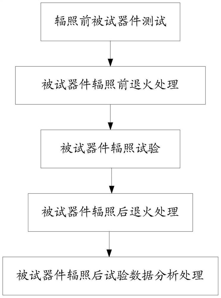
[0035] The present invention carries out the method for total dose effect test for SiC MOSFET device, such as figure 1 As shown, it includes the test of the device under test before irradiation, the second high temperature test of the device under test before irradiation, the irradiation test of the device under test, the annealing treatment of the device under test after irradiation and the analysis and processing of test data after irradiation of the device under test.

[0036] (1) Test of the device under test before exposure

[0037] According to the test conditions stipulated in the product manual, use a suitable test device to test the electrical parameters of the device under test, and record the test data. Only devices with qualified electrical parameters can be used for subsequent tests.

[0038] (2) Annealing treatment of the tested device before irradiat...


PUM


Abstract

The invention relates to a method for testing the total dose effect of a SiC MOSFET (Metal-Oxide-Semiconductor Field Effect Transistor) device, which is mainly applied to testing the total dose effect of the SiC MOSFET. According to the invention, the problem of the total dose test of the SiC MOSFET can be solved, the verification of the complex total dose effect of the SiC MOSFET is realized, in the test process, threshold voltage drift caused by total dose radiation induced defects and threshold voltage drift caused by inherent near-interface trapped charges near the SiC MOSFET interface are respectively measured, the test result is comprehensively analyzed and calculated, and the test result is accurate. According to the method, the total dose effect resistance of the SiC MOSFET device can be given, and a certain guiding effect is achieved for a user to apply anti-radiation reinforcement design and for a manufacturer to reinforce the device.

Description

technical field [0001] The invention relates to a method for testing the total dose effect of SiC MOSFET devices, and belongs to the technical field of anti-radiation of space components. Background technique [0002] Spacecraft operating in a space radiation environment will be affected by space radiation, and the total dose radiation effect in space needs to be considered, and the components in the spacecraft need to be evaluated for the total dose effect. [0003] The third generation semiconductor SiC MOSFET and Si MOSFET have similarities, both have SiO 2 The gate oxide layer has a similar total dose radiation effect caused by radiation trapping charges in the oxide layer, and there are differences, unlike SiMOSFET, which is formed by oxidation of Si to form SiO 2 Gate oxide layer, SiC MOSFET is oxidized from SiC to form SiO 2 The gate oxide layer releases C or CO during this process, forming SiO 2 / SiC interface structure and properties and SiO 2 The existence of / ...

Claims


Application Information

Patent Timeline
IPC IPC(8): G01R31/26
CPCG01R31/26Y02B70/10
Inventor 于庆奎王贺曹爽孙毅梅博吕贺莫日根王乾元孙佳佳张洪伟
Owner CHINA ACADEMY OF SPACE TECHNOLOGY
Learn More