Preparation method of quasi-two-dimensional film

A thin film preparation and thin film technology, which is applied in the field of quasi-two-dimensional thin film preparation, can solve problems such as uneven distribution of quasi-two-dimensional thin films, lower device luminous efficiency, and uneven nucleation on the thin film surface, so as to accelerate the energy transfer process and promote radiation recombination , Improve the effect of luminous efficiency

Pending Publication Date: 2022-05-13
JILIN UNIV
View PDF2 Cites 0 Cited by
  • Summary
  • Abstract
  • Description
  • Claims
  • Application Information

AI Technical Summary

Problems solved by technology

Then an appropriate amount of precursor solution is added dropwise to the surface of the substrate, followed by a spin-coating process. During the spin-coating process, at an appropriate time, an appropriate amount of non-polar solvent is quickly added dropwise to the surface of the film, thereby making the film Rapid nucleation, the nucleation completion time of the film under this process ranges from less than one second to several seconds. This rapid nucleation process will cause uneven nucleation on the surface of the film, and ultimately make the perovskite film The final shape is difficult to control, resulting in too many defects
In addition, due to the inhomogeneous nucleation of the film in this case, it is easier to cause the uneven distribution of the internal phase of the quasi-two-dimensional film during the later heating and growth process, resulting in low carrier energy transfer efficiency in the film. Reduce the luminous efficiency of the device, therefore, the preparation of quasi-two-dimensional perovskite thin films and the regulation of device performance are still facing great challenges

Method used


Image

  • Preparation method of quasi-two-dimensional film
  • Preparation method of quasi-two-dimensional film
  • Preparation method of quasi-two-dimensional film

Examples


Embodiment Construction

[0030] In order to make the object, technical solution and advantages of the present invention clearer, the present invention will be further described in detail below in conjunction with the accompanying drawings and embodiments. It should be understood that the specific embodiments described here are only used to explain the present invention, not to limit the present invention.

[0031] The specific implementation of the present invention will be described in detail below in conjunction with specific embodiments.

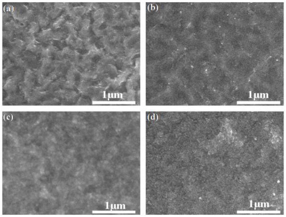
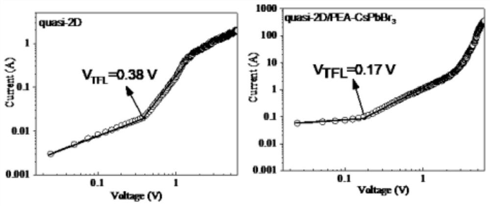
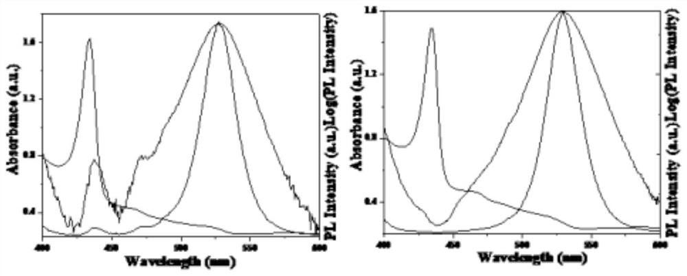
[0032] In one embodiment, a method for preparing a quasi-two-dimensional thin film, see Figure 1 ~ Figure 4 , the three-dimensional perovskite nanocrystals modified by phenethylamine are introduced into the film to regulate the radiative and non-radiative processes inside the film, thereby improving the luminescent performance of the device.

[0033] In this embodiment, the perovskite film is composed of a three-dimensional perovskite nanocrystal and a quasi-tw...


PUM


Abstract

The invention discloses a preparation method of a quasi-two-dimensional thin film, belongs to the technical field of light emitting diodes and display, solves the problems of complex process and low efficiency of the existing quasi-two-dimensional thin film preparation, and has the technical key points that a perovskite thin film is composed of three-dimensional perovskite nanocrystals and a quasi-two-dimensional perovskite thin film, wherein the surface of the three-dimensional perovskite nanocrystal is modified by an appropriate long-chain organic ligand to adapt to a cascade energy transfer process in the film, and the three-dimensional perovskite nanocrystal with a specific group is introduced into an anti-solvent, so that the nanocrystal can be used as a crystallization seed in a film preparation process to regulate and control a crystal growth kinetic process of the film, and the film is prepared. The three-dimensional perovskite nanocrystal thin film has the advantages that internal defects are passivated, the non-radiative recombination probability in the thin film is reduced, an extra carrier transmission channel from a small n phase to the three-dimensional perovskite nanocrystal can be constructed, photon-generated carrier radiative recombination is promoted, the light emission efficiency of the thin film is effectively improved, and the thin film is simple in preparation process and high in efficiency.

Description

technical field [0001] The invention relates to the technical field of light-emitting diodes and displays, in particular to a method for preparing a quasi-two-dimensional thin film. Background technique [0002] Quasi-2D metal halide perovskite materials hold great promise for light-emitting diode and display applications due to their high photoluminescence quantum yield, tunable optical bandgap, excellent color purity, and low-cost solution processability. However, the optoelectronic properties of light-emitting diodes using perovskite materials as the light-emitting layer are still far lower than those of the most advanced organic light-emitting diodes. On the one hand, it is difficult to control the crystallization process of the perovskite film solution, resulting in poor crystallization quality of the film, resulting in excessive non-radiative recombination defects; transmission efficiency. All of these will reduce the luminescent properties of the perovskite material...

Claims


Application Information

Patent Timeline
Patent Type & Authority Applications(China)
IPC IPC(8): H01L51/56C09K11/66C09K11/02
CPCC09K11/025C09K11/665H10K71/15H10K71/12H10K71/40
Inventor 张宇郜艳波白雪于伟泳陆敏武振楠暴欣宇
Owner JILIN UNIV
Why Eureka
Try Eureka