Check patentability & draft patents in minutes with Patsnap Eureka AI!

Electromigration test structure and forming method thereof, electromigration test method and memory

A test structure and electromigration technology, which is applied in semiconductor/solid-state device testing/measurement, electric solid-state devices, circuits, etc., can solve the problems of low accuracy and reliability, and achieve the effect of improving accuracy and reliability

Pending Publication Date: 2022-05-17
YANGTZE MEMORY TECH CO LTD
View PDF0 Cites 0 Cited by
  • Summary
  • Abstract
  • Description
  • Claims
  • Application Information

AI Technical Summary

Problems solved by technology

[0005] The invention provides an electromigration test structure and its forming method, and an electromigration test method, which are used to solve the problem of low accuracy and reliability of electromigration test results in the prior art

Method used


Image

  • Electromigration test structure and forming method thereof, electromigration test method and memory
  • Electromigration test structure and forming method thereof, electromigration test method and memory
  • Electromigration test structure and forming method thereof, electromigration test method and memory

Examples


Embodiment Construction

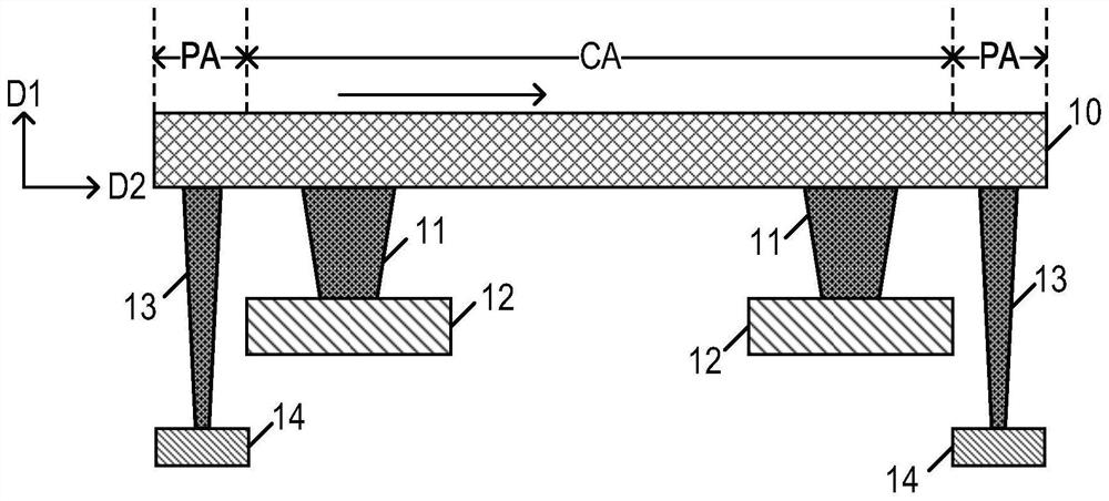
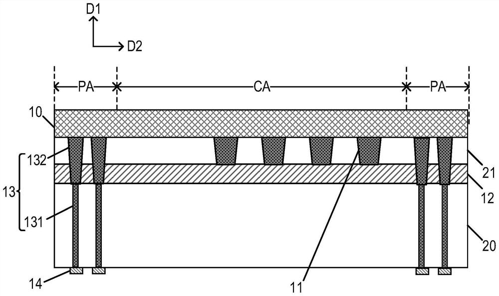
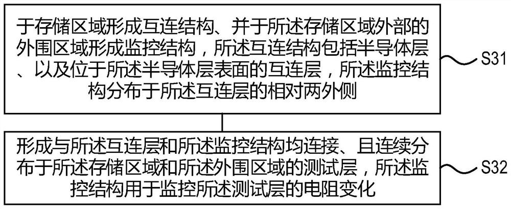
[0053] The specific implementations of the electromigration testing structure and its forming method and the electromigration testing method provided by the present invention will be described in detail below in conjunction with the accompanying drawings.

[0054] In three-dimensional memory structures such as 3D NAND memory, the well region is connected to the BTM (Bottom Top Metal, bottom top metal) through the NPU (Nwell Pick Up, N well lead-out) structure. However, the material of the NPU is usually a metal material, and the material of the well region is usually silicon, so there is a relatively large contact resistance between the NPU and the well region. When electromigration testing is currently performed on BTM, the test signal is transmitted to the BTM through the well area and the NPU, and then the resistance change is monitored through the pins drawn from the well area, that is, the BTM, NPU and BTM are currently monitored. The overall resistance of the well region...


PUM


Abstract

The invention relates to the technical field of semiconductor manufacturing, in particular to an electromigration test structure, a forming method thereof, an electromigration test method and a memory. The electromigration test structure comprises a storage area and a peripheral area located outside the storage area; the electromigration test structure further comprises test layers which are continuously distributed in the storage area and the peripheral area. The interconnection structure is located in the storage area and comprises an interconnection layer and a semiconductor layer, one end of the interconnection layer is connected with the test layer, and the other end of the interconnection layer is connected with the semiconductor layer; and the monitoring structure is located in the peripheral area, is connected with the test layer, is distributed on two opposite outer sides of the interconnection layer, and is used for monitoring the resistance change of the test layer. According to the invention, the influence of the internal resistance of the interconnection structure on the resistance monitoring of the test layer is avoided, and the accuracy and reliability of the electromigration test result are improved.

Description

technical field [0001] The invention relates to the technical field of semiconductor manufacturing, in particular to an electromigration testing structure and a forming method thereof, an electromigration testing method, and a memory. Background technique [0002] In recent years, as the size of semiconductor devices has been continuously reduced and the integration level has been continuously improved, the current of semiconductor devices during operation has been continuously increased, and the electromigration (Electromigration, EM) effect has become one of the bottlenecks for the reliability of semiconductor devices. The electromigration effect refers to the phenomenon that when the integrated circuit in the semiconductor device is working, there is a current passing through the metal wire, and the metal ion generates material transport under the action of the current. As a result, some parts of the metal line will have voids due to the electromigration phenomenon, there...

Claims


Application Information

Patent Timeline
IPC IPC(8): H01L23/544H01L21/66
CPCH01L22/34H01L22/32H01L22/14
Inventor 杨素慧杨盛玮
Owner YANGTZE MEMORY TECH CO LTD
Features
  • R&D
  • Intellectual Property
  • Life Sciences
  • Materials
  • Tech Scout
  • Unparalleled Data Quality
  • Higher Quality Content
  • 60% Fewer Hallucinations
Learn More