

Pressure sensor and preparation method thereof
A technology of pressure sensor and force sensitive resistor, which is applied in the field of pressure sensor and its preparation, can solve the problems of poor flexibility, difficult pressure accurate monitoring, strong pressure interference, etc., and achieve the effect of reducing pressure interference and improving flexibility
- Summary
- Abstract
- Description
- Claims
- Application Information
AI Technical Summary
Problems solved by technology
Method used
Image

Examples
no. 1 example
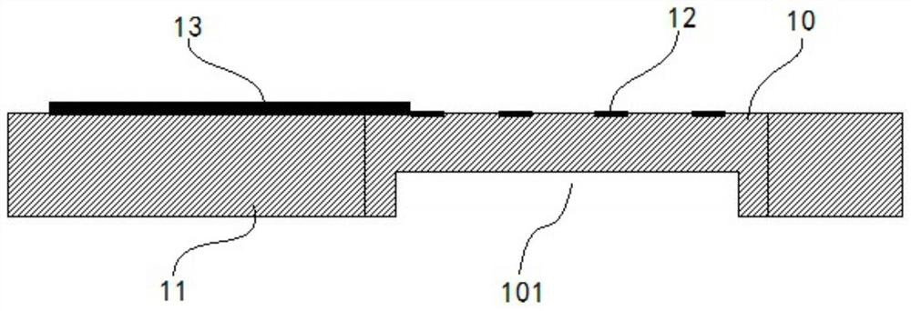
[0035] figure 1 It is a schematic structural diagram of the pressure sensor according to the first embodiment. like figure 1 As shown, the pressure sensor of this embodiment includes a silicon wafer 10 and a flexible film 11 , and at least one force-sensitive resistor 12 is disposed on one side of the silicon wafer 10 . The flexible film 11 covers the silicon wafer 10 , and the thickness of the flexible film 11 is greater than or equal to the thickness of the silicon wafer 10 .
[0036] In the present application, the force-sensitive element is embedded in the flexible film through the embedding technology. The pressure sensor thus formed has good flexibility, reduces the pressure interference of the device itself to the monitoring environment, and can realize accurate monitoring of the contact interface pressure.
[0037] In this embodiment, the silicon wafer 10 is made of SOI (Silicon-On-Insulator, silicon on insulating substrate) silicon wafer. The buried oxide layer of ...
no. 2 example
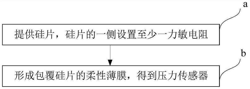
[0045] figure 2 It is a schematic flowchart of the manufacturing method of the pressure sensor according to the second embodiment. like figure 2 As shown, the preparation method of the pressure sensor in this embodiment includes the following steps:
[0046] In step a, a silicon wafer is provided, and at least one force-sensitive resistor is arranged on one side of the silicon wafer.
[0047] Optionally, in step a, including:
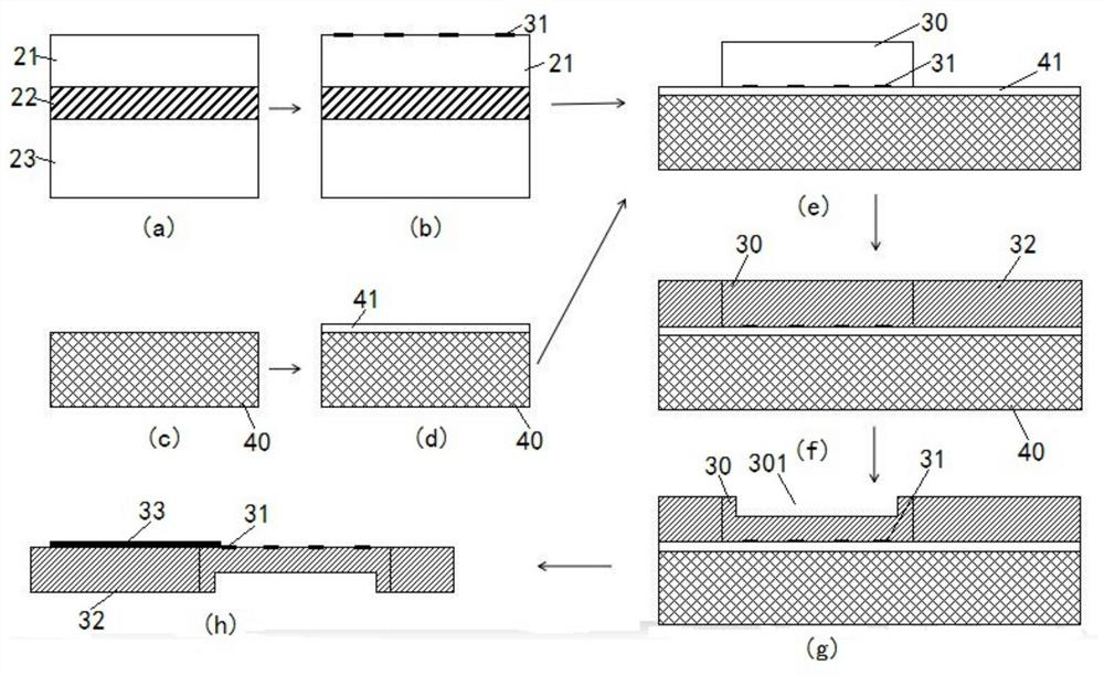
[0048] Step a1. Such as image 3 As shown in (a), an SOI silicon wafer is provided, including an upper layer of silicon 21 , a buried oxide layer 22 and a lower layer of silicon 23 . The buried oxide layer 22 separates the SOI silicon wafer into an upper layer silicon 21 and a lower layer silicon 23 .
[0049] Step a2. Such as image 3 As shown in (b), at least one force-sensitive resistor 31 is formed on one surface of the upper silicon layer 21 .
[0050] Optionally, in step a2, it also includes:
[0051] Step a21. Evenly scrape the nickel-cop...
PUM
| Property | Measurement | Unit |
|---|---|---|
| depth | aaaaa | aaaaa |
| thickness | aaaaa | aaaaa |
| thickness | aaaaa | aaaaa |
Abstract
Description
Claims
Application Information